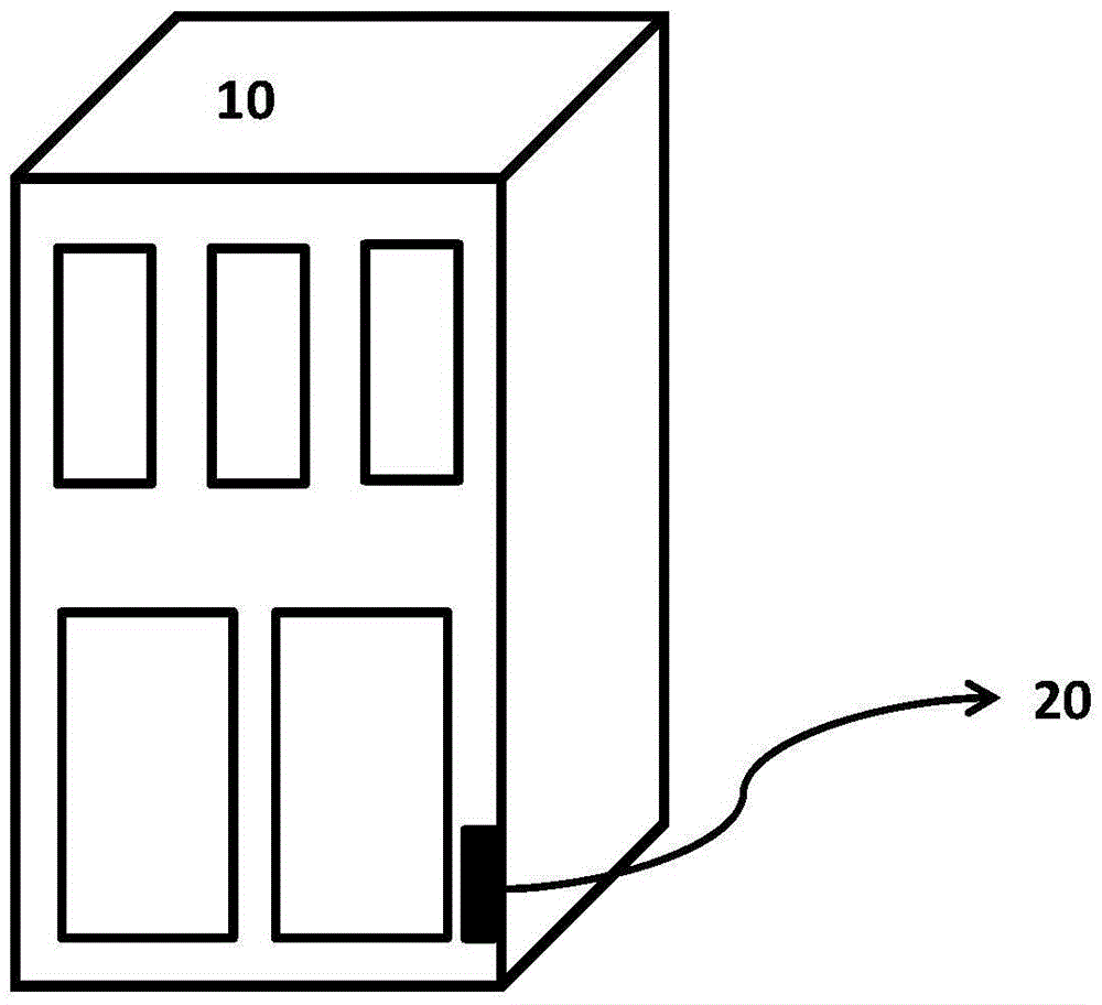
Vacuum packaging equipment based on quick response to humidity changes
A technology of vacuum packaging and humidity change, which is applied in the direction of measuring devices, instruments, and material analysis through electromagnetic means. It can solve the problems of humidity detection without pumping, increase moisture sensitivity, facilitate mass production, and promote adsorption. The effect of action
- Summary
- Abstract
- Description
- Claims
- Application Information
AI Technical Summary
Problems solved by technology
Method used
Image
Examples
Embodiment 1
[0039] A vacuum packaging equipment based on rapid response to humidity changes. The bottom of the cabinet of the vacuum packaging equipment is equipped with a humidity sensor module. The humidity sensor module includes heavily doped silicon chips arranged in sequence from bottom to top. Doped SiO 2 layer, carbon nanotube layer, on SiO 2 The lower electrode between the layers and the upper electrode on the carbon nanotube layer grown on SiO 2 layer; there is a metal film on the lower electrode, and the metal film is an adhesive Cr layer, a conductive and thermally conductive Cu layer, and an Au layer as an electrode layer from the inside to the outside, and the Cr layer, Cu layer and The thickness of the Au layer is 30nm, 300nm and 300nm in sequence; the carbon nanotube layer adopts catalyst and / or photolithography to achieve its localized growth, and the grown carbon nanotube layer adopts plasma to make it produce hydroxyl modification, The carbon nanotube layer has been tr...
Embodiment 2
[0058] A vacuum packaging equipment based on rapid response to humidity changes. The bottom of the cabinet of the vacuum packaging equipment is equipped with a humidity sensor module. The humidity sensor module includes heavily doped silicon chips arranged in sequence from bottom to top. Doped SiO 2 layer, carbon nanotube layer, on SiO 2 The lower electrode between the layers and the upper electrode on the carbon nanotube layer grown on SiO 2 layer; there is a metal film on the lower electrode, and the metal film is an adhesive Cr layer, a conductive and thermally conductive Cu layer, and an Au layer as an electrode layer from the inside to the outside, and the Cr layer, Cu layer and The thickness of the Au layer is 30nm, 400nm and 500nm in sequence; the carbon nanotube layer adopts catalyst and / or photolithography to achieve its localized growth, and the grown carbon nanotube layer is modified by plasma to produce hydroxyl groups, The carbon nanotube layer has been treated ...
Embodiment 3
[0077] A vacuum packaging equipment based on rapid response to humidity changes. The bottom of the cabinet of the vacuum packaging equipment is equipped with a humidity sensor module. The humidity sensor module includes heavily doped silicon chips arranged in sequence from bottom to top. Doped SiO 2 layer, carbon nanotube layer, on SiO 2 The lower electrode between the layers and the upper electrode on the carbon nanotube layer grown on SiO 2 layer; there is a metal film on the lower electrode, and the metal film is an adhesive Cr layer, a conductive and thermally conductive Cu layer, and an Au layer as an electrode layer from the inside to the outside, and the Cr layer, Cu layer and The thickness of the Au layer is 30nm, 260nm and 360nm in sequence; the carbon nanotube layer adopts catalyst and / or photolithography to achieve its localized growth, and the grown carbon nanotube layer is modified by plasma to produce hydroxyl groups, The carbon nanotube layer has been treated ...
PUM
| Property | Measurement | Unit |
|---|---|---|
| thickness | aaaaa | aaaaa |
| thickness | aaaaa | aaaaa |
| thickness | aaaaa | aaaaa |
Abstract
Description
Claims
Application Information

