
Mutual-capacitance embedded-type touch screen

A touch screen, mutual capacitance technology, applied in electrical digital data processing, data processing input/output process, optics, etc., can solve the problems of uniform performance degradation, low capacitance value, etc.

Active Publication Date: 2016-06-15
WUHAN CHINA STAR OPTOELECTRONICS TECH CO LTD
View PDF7 Cites 2 Cited by
  • Summary
  • Abstract
  • Description
  • Claims
  • Application Information

AI Technical Summary

Problems solved by technology

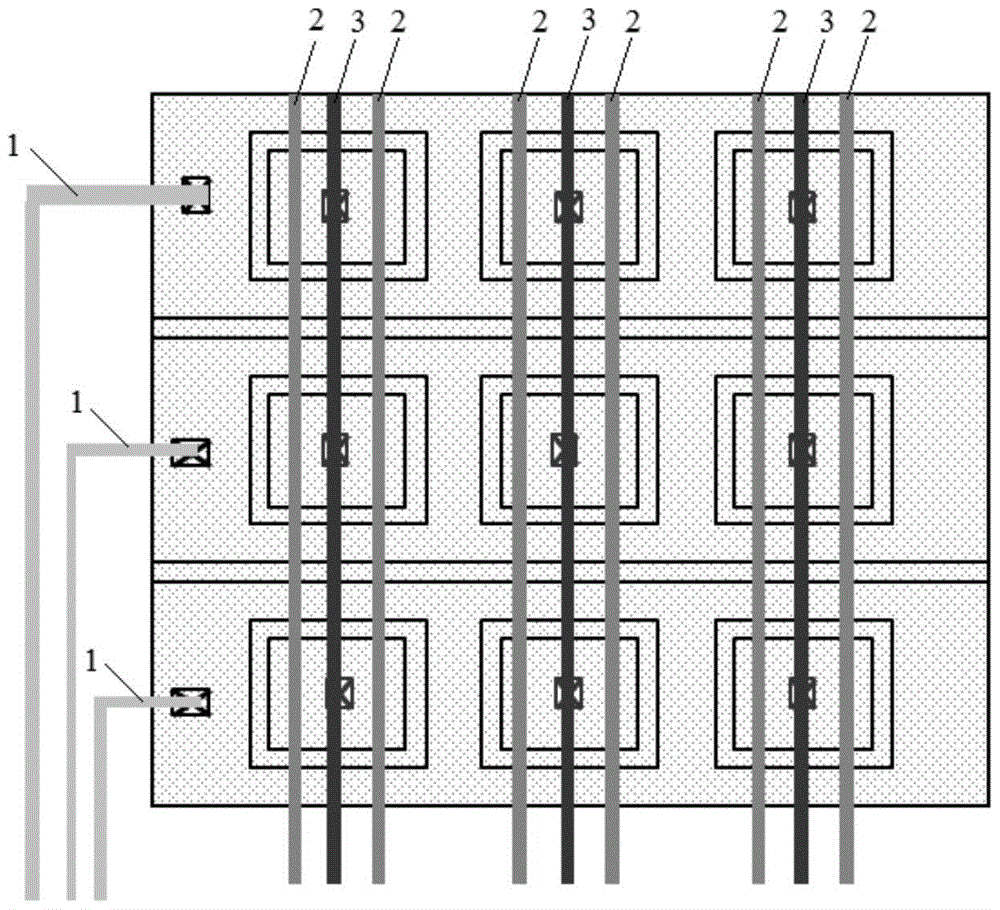
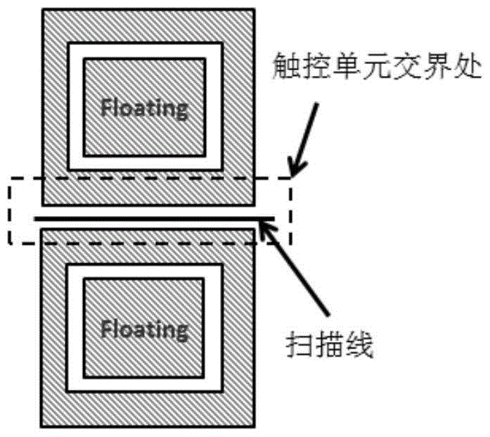
[0004] figure 1 Shows the planar layout of the embedded capacitive screen of the existing Incell structure, such as figure 1 As shown, 1 is the driving signal supply wiring, 2 is the touch sensing electrode, 3 is the common signal supply wiring, figure 2 shown as figure 1 The floor plan of two adjacent touch units in , by figure 2 It can be seen that there is a gap at the junction of two adjacent touch units, and the scanning line at the junction does not overlap with the common electrode layer, resulting in a low capacitance value, while the scanning line at the non-junction and the common electrode layer do not overlap. There is overlap in the common electrode layer, and its capacitance value is high, which leads to a decrease in the uniform performance of the embedded capacitive screen of the existing Incell structure in terms of display, that is, at the junction of two adjacent touch units Visible streaks appear

Method used


Image

  • Mutual-capacitance embedded-type touch screen
  • Mutual-capacitance embedded-type touch screen
  • Mutual-capacitance embedded-type touch screen

Examples


Embodiment Construction

[0024] Reference will now be made in detail to exemplary embodiments of the present invention, examples of which are illustrated in the accompanying drawings. The embodiments are described below to explain the present invention by referring to the figures. This invention may, however, be embodied in many different forms and should not be construed as limited to the exemplary embodiments set forth herein. Rather, these embodiments are provided so that this disclosure will be thorough and complete, and will fully convey the scope of the invention to those skilled in the art.

[0025] For clarity and conciseness, descriptions of unnecessary parts or elements may be omitted, and like reference numerals denote like elements throughout. In the drawings, the size and relative sizes of layers and regions, and the distance and relative distance between elements may be exaggerated for clarity. Therefore, the drawings only schematically show the relative positional relationship among t...


PUM


Abstract

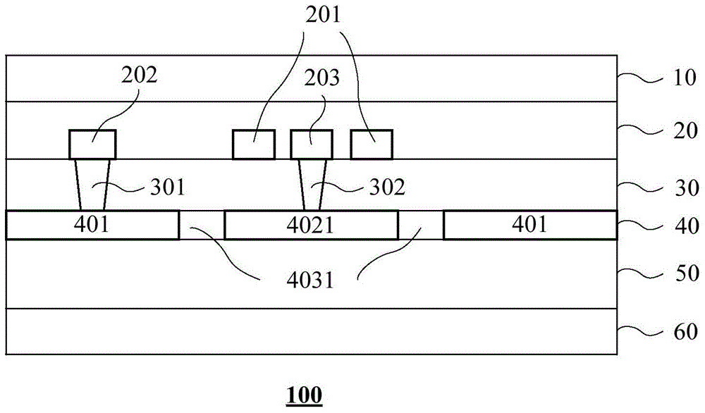
A mutual-capacitance embedded-type touch screen is provided. The embedded-type touch screen comprises a touch control unit array formed by a plurality of touch control units. The mutual-capacitance embedded-type touch screen is characterized in that each touch control unit is formed by a pixel electrode layer, a first dielectric layer, a second dielectric layer, a common electrode layer, a third dielectric layer and a thin film transistor array which are stacked in order. The common electrode layer of each touch control unit is divided into a driving area, a first suspension area, a second suspension area, a first shielding area and a second shielding area, the first shielding area and the second shielding area are respectively formed at two sides, which are back to each other, of the driving area, the first suspension area is formed at one side, of the first shielding area, being far from the driving area, and the second suspension area is formed at one side, of the second shielding area, being far from the driving area. With respect to the mutual-capacitance embedded-type touch screen, the capacitance value of a scan line on the juncture of adjacent touch control units is approximate to that of a scan line which is not positioned on the juncture, and the case that obvious stripes occur on the juncture of adjacent touch control units can be effectively avoided.

Description

technical field [0001] The present invention generally relates to the structure of an in-cell touch screen, and more specifically, relates to a mutual-capacitance in-cell (Incell) touch screen. Background technique [0002] With the continuous development of electronic science and technology, capacitive touch screens (hereinafter referred to as "capacitive screens") are widely used in various electronic devices, such as: smart phones, tablet computers, game consoles, personal digital assistants and other electronic devices with touch screens. equipment. The existing capacitive screen structures include external capacitive screens represented by G+G, GF, GFF, OGS, etc., and embedded capacitive screens represented by Oncell and Incell. [0003] In recent years, people are pursuing more and more light and thin user experience, and there has been a situation where OGS, Oncell, and Incell are competing with each other. Due to the unique advantages in the production process, Ince...

Claims


Application Information

Patent Timeline
IPC IPC(8): G06F3/041G06F3/044
CPCG06F3/0412G06F3/044G06F2203/04107G06F3/0443G06F3/0446G06F2203/04112G02F1/134318
Inventor 谢剑星蔡育徵黄俊宏
Owner WUHAN CHINA STAR OPTOELECTRONICS TECH CO LTD
Learn More