Laminate for light emitting device and process of preparing same

A light-emitting device and stacking technology, which is applied in the semiconductor devices of light-emitting elements, semiconductor/solid-state device manufacturing, and electric solid-state devices, etc., can solve the problems of loss of optical properties of light-emitting devices and increase of bubble concentration

Inactive Publication Date: 2016-06-15
SAINT-GOBAIN GLASS FRANCE
View PDF14 Cites 6 Cited by
  • Summary
  • Abstract
  • Description
  • Claims
  • Application Information

AI Technical Summary

Problems solved by technology

However, there is still the following problem: forming a stable raised structure with a high tilt angle requires the thickness of the planar layer to be at least twice the height of the raised structure to completely cover the raised structure
[0018] Further, when a glass frit is used as a raw material for a flat layer, a problem has been found that the concentration of trapped air bubbles generated during firing of the frit increases as the thickness increases
In this regard, there is still a risk of gas bubbles being trapped in the inner light extraction layer during sintering, which causes a loss of optical properties of the light emitting device due to an increase in the light path

Method used


Image

  • Laminate for light emitting device and process of preparing same
  • Laminate for light emitting device and process of preparing same
  • Laminate for light emitting device and process of preparing same

Examples


example 1

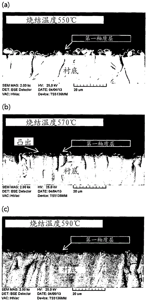
[0172] Example 1: Fabrication of stacks for light emitting devices

[0173] Prepared as follows: a soda lime glass substrate having a thickness of 0.7 mm; a first glass frit paste comprising (based on the total weight of the paste) 20% by weight of a glass frit comprising 28.4% by weight of SiO 2 , 3.6% Al by weight 2 o 3 , 39.5% by weight of B 2 o 3 , 11.6% by weight of ZnO, 3% by weight of P 2 o 5 and (based on the total weight of the first glass frit paste) by weight 13.9% Na 2 O, and (based on the total weight of the paste) 80% by weight of ethyl cellulose as a binder and diethylene glycol butyl ether acetate as a solvent; and a second glass frit paste comprising (based on the total weight of the paste of) 75% by weight of glass frit which includes 70% by weight of Bi 2 o 3 , 10% by weight ZnO, 3% by weight Al 2 o 3 , 7% SiO by weight 2 , 9% by weight of B 2 o 3 and (based on the total weight of the second glass frit paste) by weight 1% Na 2 O and (based on...


PUM

PropertyMeasurementUnit
thicknessaaaaaaaaaa
surface roughnessaaaaaaaaaa
thicknessaaaaaaaaaa

Abstract

The present invention relates to a laminate for a light emitting device, comprising a glass substrate, a random network of reliefs formed on the glass substrate, and a flattening layer formed on the network, wherein the network of reliefs are formed from a glass frit. The laminate for a light emitting device according to the invention is characterized by comprising a network inducing the scattering of light for efficiently extracting outward a loss of light at an interface between a glass substrate and an internal light extraction layer. The laminate is suitable for the industrial field of optical devices, such as organic light emitting diodes (OLEDs), backlights, lighting, and the like.

Description

technical field [0001] The present invention relates to a stack for a light emitting device and a process for preparing the stack for enhancing external light by minimizing loss of light at the interface between a glass substrate and an internal light extraction layer efficiency. The laminate used for the light-emitting device of the present invention is particularly suitable for the industrial field of optical devices such as organic light-emitting diodes (OLEDs), backlights and lighting, and the like. Background technique [0002] Depending on the emission structure, optical devices such as OLEDs can be classified into bottom emission structures in which light is emitted toward a glass substrate and top emission structures in which light is emitted in the opposite direction to the glass substrate. In the bottom emission structure, the cathode serves as a reflector by using a metal thin film of aluminum or the like, and the anode serves as a path for light emission by usin...

Claims


Application Information

Patent Timeline
Patent Type & Authority Applications(China)
IPC IPC(8): H01L51/52H01L51/56
CPCY02E10/549F21K9/60F21V5/002Y02B20/30Y02P70/50H10K77/10H10K50/854H10K50/844H10K50/858H10K50/85H10K2102/351H10K71/00C03B23/20H10K50/81H10K50/828H10K50/856H10K2102/00F21K9/90
Inventor 李荣盛韩镇宇
Owner SAINT-GOBAIN GLASS FRANCE
Why Eureka
Try Eureka