Array substrate and manufacturing method thereof and display device

An array substrate and substrate technology, applied in optics, instruments, electrical components, etc., can solve the problems of increasing power consumption of array substrates

Inactive Publication Date: 2016-07-06
BOE TECH GRP CO LTD
View PDF3 Cites 9 Cited by
  • Summary
  • Abstract
  • Description
  • Claims
  • Application Information

AI Technical Summary

Problems solved by technology

[0004] At present, the existing solution is to increase the gate-source capacitance of the pixel electrode farther from the gate drive signal input end of the gate line, so as to increase the capacitance of the pixel el

Method used


Image

  • Array substrate and manufacturing method thereof and display device

Examples


Embodiment Construction

[0023] In order to understand the above-mentioned purpose, features and advantages of the present invention more clearly, the present invention will be further described in detail below in conjunction with the accompanying drawings and specific embodiments. It should be noted that, in the case of no conflict, the embodiments of the present application and the features in the embodiments can be combined with each other.

[0024] In the following description, many specific details are set forth in order to fully understand the present invention. However, the present invention can also be implemented in other ways different from those described here. Therefore, the protection scope of the present invention is not limited by the specific details disclosed below. EXAMPLE LIMITATIONS.

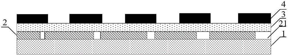
[0025] In a first aspect, the present invention provides an array substrate. The array substrate includes a base, and further includes a common electrode formed on the base, a plurality of rows of ga...


PUM


Abstract

The invention relates to an array substrate and a manufacturing method thereof and a display device. The array substrate comprises a substrate, common electrodes, multiple rows of grid lines and multiple pixel electrodes, wherein the common electrodes, the multiple rows of grid lines and the multiple pixel electrodes are formed on the substrate; the pixel electrodes and the common electrodes are arranged at different layers; a vertical overlap part exists in each pixel electrode and the corresponding common electrode; and in two pixel electrodes connected to the same row of grid lines, the area of the vertical overlap part of the pixel electrode which is further to the first ends of the grid lines and the corresponding common electrode is smaller than that of the pixel electrode which is nearer the first ends of the grid lines and the corresponding common electrode. According to the array substrate, the leaping voltage of the pixel electrode further to the first ends of the grid lines obtains more compensation than that nearer the first ends of the grid lines, so that the difference between the leaping voltages of two pixel electrodes is reduced; the residual image is reduced. Furthermore, compared with the mode of increasing a gate-source capacitance in the prior art, the array substrate has the advantage that the power consumption of the array substrate can be reduced.

Description

technical field [0001] The present invention relates to the field of display technology, in particular to an array substrate, a manufacturing method thereof, and a display device. Background technique [0002] Thin Film Transistor Liquid Crystal Display (TFT-LCD for short) has the characteristics of small size, low power consumption, and no radiation, and occupies a dominant position in the current flat panel display market. [0003] In the TFT-LCD of the prior art, a jump voltage ΔVp is generated on the pixel electrode at the moment when the charging of the pixel electrode ends. Since the delay of the gate driving signal is different at different positions on a row of gate lines, the jump voltage ΔVp generated on the pixel electrodes connected to different positions on a row of gate lines is different, and the distance from the grid line to the gate line is different. The farther the pixel electrode is from the input terminal of the pole driving signal, the smaller the jum...

Claims


Application Information

Patent Timeline
IPC IPC(8): H01L27/12G02F1/1362
CPCG02F1/136213H01L27/124H01L27/1259
Inventor 张慧
Owner BOE TECH GRP CO LTD
Why Eureka
Try Eureka