Silicon ingot and preparation method thereof

A silicon ingot and silicon material technology, applied in the field of solar cell materials, can solve problems such as uneven distribution of resistivity of silicon ingots

Inactive Publication Date: 2016-07-20
JIANGSU XIEXIN SILICON MATERIAL TECH DEV
View PDF7 Cites 4 Cited by
  • Summary
  • Abstract
  • Description
  • Claims
  • Application Information

AI Technical Summary

Problems solved by technology

[0004] Based on this, it is necessary to provide a method for preparing silicon ingots that makes the resistivity distribution of silicon ingo

Method used


Image

  • Silicon ingot and preparation method thereof

Examples


preparation example Construction

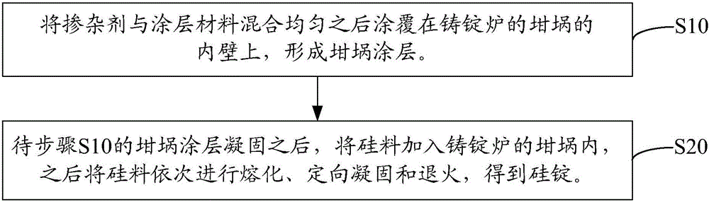
[0023] like figure 1 Shown, the preparation method of the silicon ingot of one embodiment, comprises the steps:

[0024] S10, uniformly mixing the dopant and the coating material and then coating the inner wall of the crucible of the ingot furnace to form a crucible coating.

[0025] The quality of the dopant depends on the target resistivity of the silicon ingot. For example, if the target resistivity of the boron-doped silicon ingot is 1.7Ω, the mass ratio concentration of boron is calculated to be 70ppbw. If the mass of the silicon material in the crucible is 850kg, Then the mass of boron element required is 0.06g. The photoelectric performance of the prepared silicon ingot can be better controlled by precise calculation.

[0026] The dopant is selected from at least one of a master alloy and a semiconductor element. The master alloy is an alloy of impurity elements and silicon. In a preferred embodiment, the master alloy is selected from at least one of gallium-silicon ...

Embodiment 1

[0042]18g of gallium, 620g of silicon nitride, 350ml of silica sol, 50g of binder and 1200ml of pure water were mixed and stirred evenly, and then sprayed on the inner wall of the crucible of the ingot furnace to form a crucible coating.

[0043] After the coating of the crucible is solidified, add 850kg of silicon material into the crucible, and then put the crucible filled with silicon material into the ingot furnace.

[0044] Vacuum the ingot furnace, then heat the silicon material to 1175°C, maintain the pressure in the ingot furnace at 600mbar, and then raise the temperature to 1510°C to melt the silicon material from top to bottom.

[0045] After the silicon material is melted, it enters the crystal growth stage, and the silicon ingot is directional solidified from bottom to top by opening the steel cage and lowering the temperature in the furnace.

[0046] After the crystal growth is completed, the silicon ingot of Example 1 can be obtained after annealing and cooling. ...

Embodiment 2

[0059] 200g of borosilicate alloy (containing 0.06g of boron), 620g of silicon nitride, 330ml of silica sol, 45g of binder and 1100ml of pure water were mixed and stirred evenly, and then sprayed on the inner wall of the crucible of the ingot furnace to form a crucible coating.

[0060] After the coating of the crucible is solidified, the silicon material is added into the crucible of the ingot furnace, and then the crucible filled with the silicon material is put into the ingot furnace.

[0061] Vacuum the ingot furnace, then heat the silicon material to 1160°C, maintain the pressure in the ingot furnace at 600mbar, and then raise the temperature to 1535°C to melt the silicon material from top to bottom.

[0062] After the silicon material is melted, it enters the crystal growth stage, and the silicon ingot is directional solidified from bottom to top by opening the steel cage and lowering the temperature in the furnace.

[0063] After the crystal growth is completed, the sil...


PUM

PropertyMeasurementUnit
Thicknessaaaaaaaaaa

Abstract

The invention relates to a silicon ingot and a preparation method thereof. The preparation method of the silicon ingot comprises the following steps: uniformly mixing dopants with coating materials and then coating the inner wall of a crucible of an ingot furnace with the mixture, thus forming a crucible coating; and after the crucible coating is solidified, adding silicon materials to the crucible of the ingot furnace and then carrying out melting, directional solidification and annealing on the silicon materials in sequence, thus obtaining the silicon ingot. In the preparation method of the silicon ingot, firstly the dopants are uniformly mixed with the coating materials and the inner wall of the crucible is coated with the mixture, and then at the silicon material melting stage, a small number of dopants enter the silicon liquid obtained after melting to be fused with the silicon liquid to undergo segregation; and the directional solidification process is the crystal growth stage and plenty of dopants on the inner wall of the crucible can diffuse in the silicon ingot, so that segregation of the dopants can be reduced and the resistivity of the silicon ingot can be effectively controlled, thus enabling the resistivity of the silicon ingot to be uniform in distribution, increasing the yield of the cast ingot and effectively reducing the cost. Besides, the invention also relates to the silicon ingot prepared by the preparation method.

Description

technical field [0001] The invention relates to the field of solar cell materials, in particular to a silicon ingot and a preparation method thereof. Background technique [0002] Since entering this century, the photovoltaic industry has become the fastest growing high-tech industry in the world. Among all kinds of solar cells, crystalline silicon cells occupy more than 75% of the market share. How to further improve the conversion efficiency of crystalline silicon cells will play a vital role in the development of the photovoltaic industry. [0003] At present, silicon wafers for solar cells are processed from silicon ingots. In order to meet the requirements of cell processing, silicon ingots must be added with master alloy dopants during the crystal growth process, and their concentration must be adjusted to obtain the required electrical properties. However, in the traditional silicon ingot preparation method, the master alloy is directly added to the silicon material,...

Claims


Application Information

Patent Timeline
IPC IPC(8): C30B29/06C30B11/00C30B28/06
CPCC30B29/06C30B11/00C30B28/06
Inventor 居发亮吴义华武鹏郭晓琛黄春来汪晨
Owner JIANGSU XIEXIN SILICON MATERIAL TECH DEV
Why Eureka
Try Eureka