Voltage-controlled semiconductor construction, resistor, and method for manufacturing same

A technology for voltage control and resistors, applied in semiconductor/solid-state device manufacturing, semiconductor devices, electric solid-state devices, etc., can solve the problems of large size of resistors and inability to adjust resistivity

Inactive Publication Date: 2007-08-22
SYST GEN
View PDF0 Cites 0 Cited by
  • Summary
  • Abstract
  • Description
  • Claims
  • Application Information

AI Technical Summary

Problems solved by technology

However, the fabricated resistor size is still large
[0004] Both approaches have another common disadvantage, that is, once the two resistors are manufactured, their resistivity cannot be adjusted.
[0005] In summary, there are critical problems in both of the current approaches, thus limiting the application of resistors in circuit systems

Method used


Image

  • Voltage-controlled semiconductor construction, resistor, and method for manufacturing same
  • Voltage-controlled semiconductor construction, resistor, and method for manufacturing same
  • Voltage-controlled semiconductor construction, resistor, and method for manufacturing same

Examples


no. 1 Embodiment

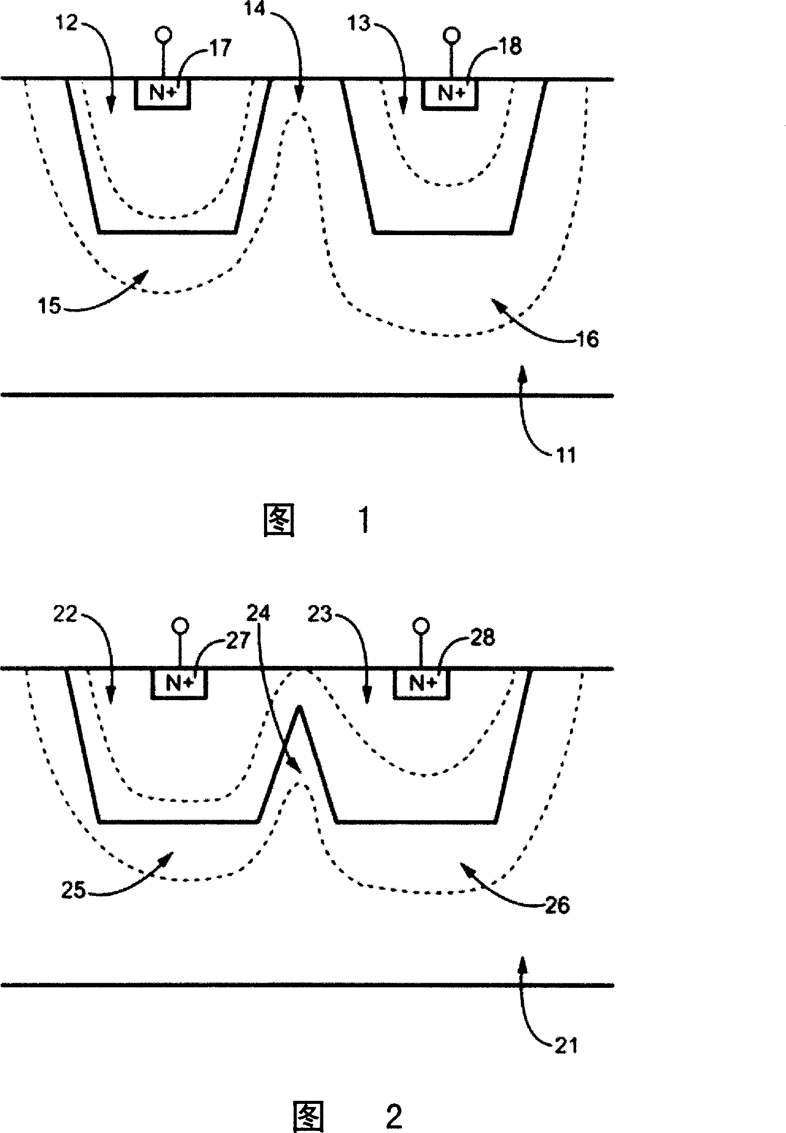
[0018] Figure 1 shows a first embodiment of the invention, which is a voltage controlled resistor. The resistor comprises a P substrate 11 and two deep N well regions 12 and 13 . Two N+ regions 17 and 18 are respectively formed in the two deep N well regions 12 and 13 as terminals of the resistor. The two deep N well regions 12 and 13 are formed on the P substrate 11 and are split. An equivalent resistor 14 is formed between the two deep N-well regions 12 and 13 . A depletion region 15 is formed between the deep N-well region 12 and the P-substrate 11 , the boundary of which is shown by two dashed lines. Similarly, a depletion region 16 is formed between the deep N well region 13 and the P substrate 11 , the boundary of which is shown by two dotted lines. The two depletion regions 15 and 16 are connected.

[0019] Through these N+ regions 17 and 18, a differential voltage is applied to the resistor, and between the P-type doped regions such as the P substrate 11 and the N-...

no. 3 Embodiment

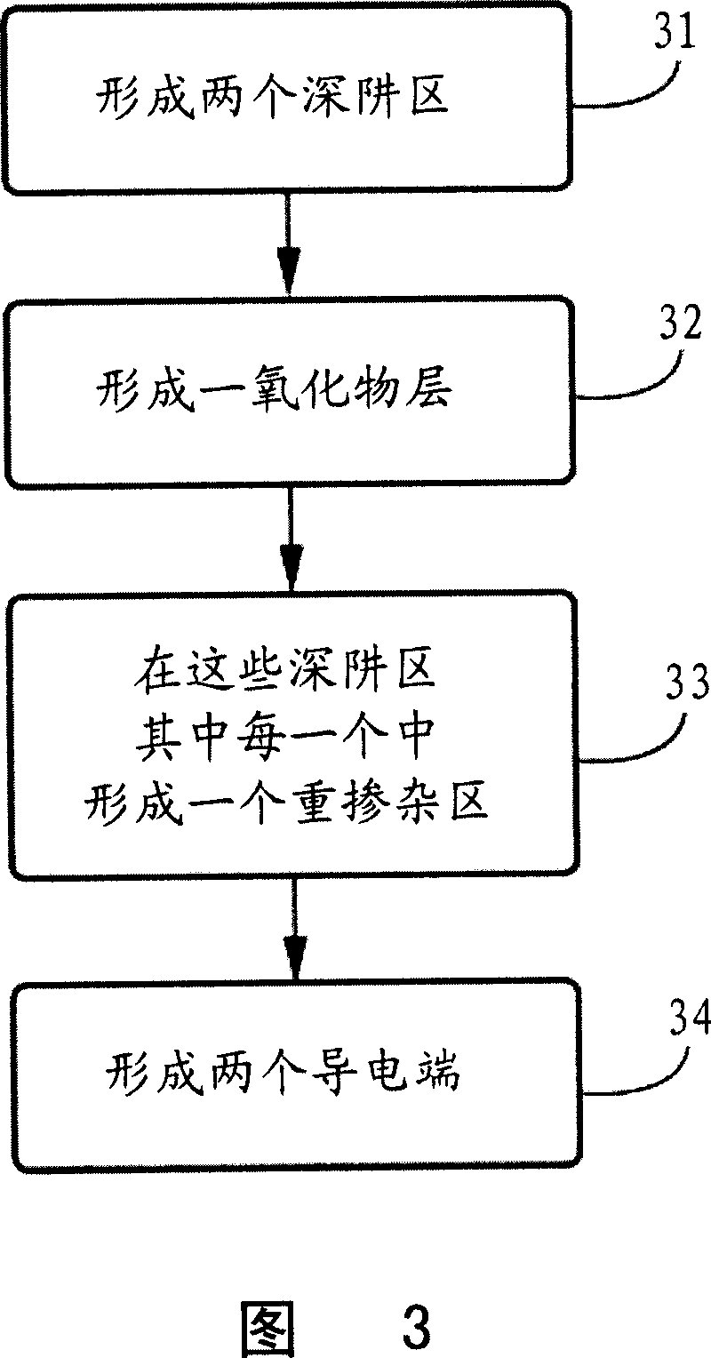
[0026] In a third embodiment of the present invention, a semiconductor structure has an equivalent resistor area substantially equal to that of the first and second embodiments. The third specific embodiment includes a substrate and a deep well region formed in the substrate and has a gap, which means that the third specific embodiment is to apply the process of manufacturing the deep well region with a gap to realize the first The penetrating structure of a specific embodiment or the clamping structure of the second specific embodiment. The ion types of the substrate and the deep well region are complementary. Between the deep well region and the substrate, a depletion region is changed according to a voltage applied to the deep well region to control the resistivity of the semiconductor structure. When forming the penetrating structure and the pinching structure, a single photomask process is used to form the deep well region, which means that the process of forming the dee...


PUM


Abstract

The invention provides a voltage-controlled semiconductor structure, a voltage-controlled resistor and a manufacturing method thereof. The semiconductor structure comprises a substrate, a first adulteration trap and a second adulteration trap. The substrate is adulterated with a first type ion. The first adulteration trap has a second type ion and is formed in the substrate. The second adulteration trap has a second type ion and is formed in the substrate. The first type ion and the second type ion are inter-complementary. A resistor is formed between the first adulteration trap and the second adulteration trap. The electrical resistivity of the resistor is controlled by a differential voltage. An electrical resistivity of the resistor is related to a first deepness of the first adulteration trap, a second deepness of the second adulteration trap and a distance between the first adulteration trap and the second adulteration trap. The electrical resistivity of the resistor is higher than an electrical resistivity of a trap type resistor formed in a single adulteration trap having the second type ion.

Description

technical field [0001] The invention relates to a voltage-controlled semiconductor structure, a resistor and a manufacturing method thereof, more specifically, a voltage-controlled semiconductor structure, a resistor with high resistivity and a manufacturing method thereof. Background technique [0002] Resistors with high resistivity are widely used in many electronic products. Today, there are two main approaches to fabricate resistors with high resistivity. One is to use undoped polysilicon as the resistor. The resistivity of this type of resistor is about 1 kohm / unit area. The advantage of this approach is that the resistors it produces are smaller in size. However, additional photomasks and processes are used in its manufacturing process, which is costly. [0003] Another approach is to make the resistor with a slightly doped well region. The highest resistivity of resistors fabricated in this way is about 10 kohms / unit area. Since a resistor with a well region ha...

Claims


Application Information

Patent Timeline
Patent Type & Authority Applications(China)
IPC IPC(8): H01L27/04H01L27/00H01L21/822
CPCH01L29/8605H01L29/66166
Inventor 蒋秋志黄志丰
Owner SYST GEN
Why Eureka
Try Eureka