Growing method of monocrystalline silicon and monocrystalline silicon

A growth method, single crystal silicon technology, applied in the direction of single crystal growth, single crystal growth, crystal growth, etc., can solve problems such as difficulty in accurate prediction of dopant concentration, reduction of crystal ratio, deviation of crystal resistivity, etc.

Active Publication Date: 2021-04-20
杭州晶宝新能源科技有限公司
View PDF10 Cites 1 Cited by
  • Summary
  • Abstract
  • Description
  • Claims
  • Application Information

AI Technical Summary

Problems solved by technology

During the complete cycle of the crucible, due to the complex growth program and growth parameters such as furnace chamber pressure, temperature, time, etc., the volatilization of dopant atoms is significantly affected, making it extremely difficult to accurately predict the dopant concentration in the melt
The deviation of dopant concentration will cause the actual resistivity of the crystal to deviate from the target value, reducing the proportion of compliant crystals

Method used


Image

  • Growing method of monocrystalline silicon and monocrystalline silicon
  • Growing method of monocrystalline silicon and monocrystalline silicon
  • Growing method of monocrystalline silicon and monocrystalline silicon

Examples


Embodiment 1

[0040] This embodiment proposes a method for growing single crystal silicon, comprising the following steps:

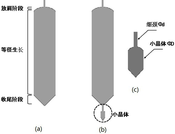
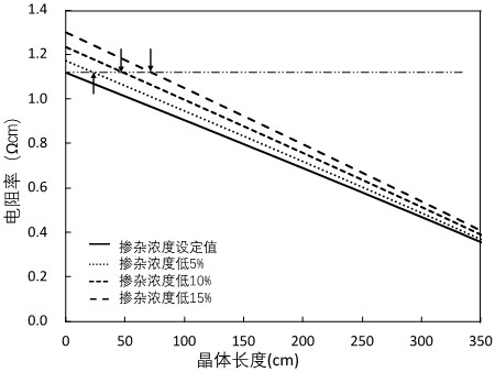
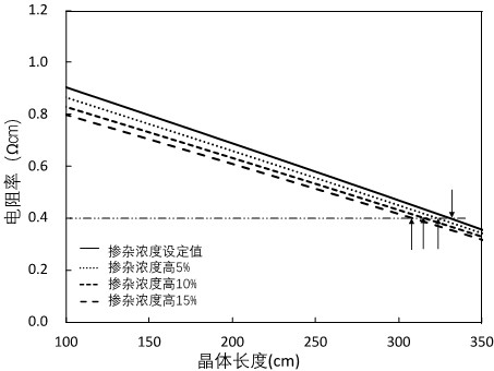
[0041] A single crystal silicon crystal with a diameter of 262 mm was grown by the Chess pulling method. 600kg of high-purity polysilicon is loaded into a high-purity quartz crucible, the design resistivity of the head is 1.1Ωcm, and 49.2g of high-purity metal gallium (dopant) is added. Under the protection of inert gas, the raw materials are melted to obtain a stable melt. Enter the seeding, necking, shouldering and equal-diameter growth procedures, and enter the finishing procedure when the crystal length is controlled to be about 330cm (the tail resistivity is about 0.4Ω㎝). At the end of the finishing stage, the temperature of the melt was increased, and the crystal pulling speed was increased to form a thin neck with a diameter of about 3 mm. When the thin neck grows stably at about 20mm, a small crystal with a diameter of 25.4mm is grown on the shoulder, and when...


PUM


Abstract

The invention discloses a growth method of monocrystalline silicon and monocrystalline silicon, and belongs to the technical field of monocrystalline silicon. The growth method of the monocrystalline silicon comprises the following steps of: putting a set amount of polycrystalline silicon raw material and a dopant into a growth container; carrying out crystal growth by adopting a pulling method; continuously growing a to-be-detected crystal at the last stage of an ending stage; calculating the concentration of the dopant in the remainder of the growth container by testing the resistivity of the to-be-detected crystal; and calculating the supplement amount of the dopant according to the concentration of the dopant in the remainder so as to supplement the concentration of the dopant to a set value for the growth of the next crystal. According to the method, the concentration of the dopant in the remainder can be more accurately tested, the concentration of the dopant in the growth container before the next crystal grows can be accurately controlled, the resistivity of the crystal can be more accurately controlled, the resistivity of the crystal is prevented from deviating from a target value to a certain extent, and the product percent of pass is increased.

Description

technical field [0001] The invention relates to the technical field of single crystal silicon, in particular to a method for growing single crystal silicon and single crystal silicon. Background technique [0002] At present, the Czochralski (Czochralski) pulling method is the mainstream method for preparing single crystal silicon crystals. In this method, high-purity polysilicon raw materials are added to a quartz crucible for melting, and seed crystals are used to seed crystals, and the crystals are gradually extracted from the melt through precise control. Large-sized single crystals grow. The growth procedure includes seeding, necking, shouldering, isometric growth and finishing procedures, and the complete process takes tens of hours. [0003] In order to reduce production costs, the industry usually refills polysilicon raw materials in the crucible after growing a crystal to grow new crystals, so as to increase the utilization times of the crucible, so that the servic...

Claims


Application Information

Patent Timeline
IPC IPC(8): C30B15/04C30B15/20C30B29/06
Inventor 陈鹏李晓强
Owner 杭州晶宝新能源科技有限公司
Why Eureka
Try Eureka