Curved-surface liquid crystal display panel and production method thereof

A technology of liquid crystal display panel and manufacturing method, which is applied in the direction of nonlinear optics, instrumentation, optics, etc., can solve the problems of uneven thickness of liquid crystal panel box, Mura, frame glue fracture, etc., achieve effective dispersion of shear stress, and simple manufacturing method , the effect of uniform box thickness

Active Publication Date: 2016-07-20
SHENZHEN CHINA STAR OPTOELECTRONICS TECH CO LTD
View PDF5 Cites 29 Cited by
  • Summary
  • Abstract
  • Description
  • Claims
  • Application Information

AI Technical Summary

Problems solved by technology

[0004] However, in the process of making a curved display, after the curved surface is formed, since the upper and lower substrates are based on the center of the panel, there will be a relative shift (shift) to the left and right sides in the horizontal direction, which will cause the dislocation of the PS, and the PS will move into the TFT array. In the channel on the substrate si...

Method used


Image

  • Curved-surface liquid crystal display panel and production method thereof
  • Curved-surface liquid crystal display panel and production method thereof
  • Curved-surface liquid crystal display panel and production method thereof

Examples


Embodiment Construction

[0041]In order to further illustrate the technical means and effects adopted by the present invention, the following describes in detail in conjunction with preferred embodiments of the present invention and accompanying drawings.

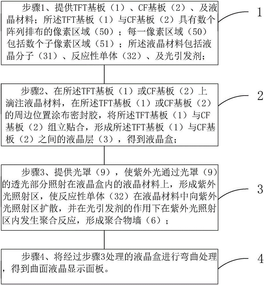
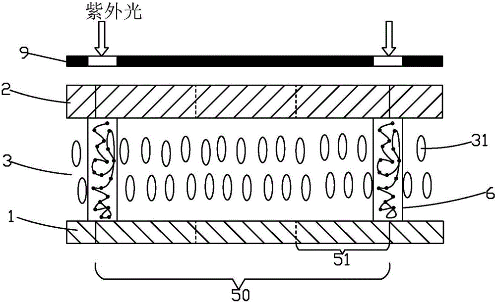
[0042] see figure 1 , the invention provides a method for manufacturing a curved liquid crystal display panel, comprising the following steps:

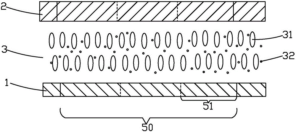
[0043] Step 1. Provide a TFT substrate 1, a CF substrate 2, an alignment film material, and a liquid crystal material; apply an alignment film material on the opposite side of the TFT substrate 1 and the CF substrate 2, and perform rubbing alignment or optical alignment. For alignment, an alignment film (not shown) is formed on one side of the TFT substrate 1 and the CF substrate 2 .

[0044] Specifically, both the TFT substrate 1 and the CF substrate 2 have a plurality of pixel regions 50 arranged in an array corresponding to each other; each pixel region 50 includes a plurality of sub-pixel regions 51 ....


PUM


Abstract

The invention provides a curved-surface liquid crystal display panel and a production method thereof. According to the production method, reaction monomers mixed in a liquid crystal material form a polymer wall at the edge of each corresponding pixel region between a TFT substrate and a CF substrate or the edge of each subpixel region by virtue of a photomask under the irradiation of ultraviolet light; compared with traditional partitions, the polymer walls are uniformly distributed on each pixel, so that the relatively uniform box thickness of a panel can be guaranteed during bending; meanwhile, the shearing stress between the TFT substrate and the CF substrate is effectively dispersed by virtue of the uniformly distributed polymer walls, so that a frame sealant can be protected from being damaged; and besides, compared with a method for forming the partitions by virtue of photoresistance photoetching, the production method has the advantages that the polymer walls are generated by virtue of in-situ reaction in a liquid crystal box, so that the problem that the box thickness is not uniform due to alignment deviation or terrain deviation is avoided.

Description

technical field [0001] The invention relates to the field of display technology, in particular to a method for manufacturing a curved liquid crystal display panel and the curved liquid crystal display panel. Background technique [0002] A liquid crystal display (LiquidCrystalDisplay, LCD) includes a housing, a liquid crystal panel disposed in the housing, and a backlight module disposed in the housing, wherein the liquid crystal panel consists of a color filter substrate (ColorFilterSubstrate, CFSubstrate), a thin film transistor array substrate (ThinFilmTransistorArraySubstrate, TFTArraySubstrate), and the liquid crystal layer (LiquidCrystalLayer, LC) sandwiched between the CF substrate and the TFT array substrate and the sealant (Sealant). There are transparent electrodes on the opposite inner sides of the CF substrate and the TFT substrate. The liquid crystal display controls the orientation of the liquid crystal molecules through the electric field, changes the polariza...

Claims


Application Information

Patent Timeline
IPC IPC(8): G02F1/1339G02F1/1333
CPCG02F1/1333G02F1/13394G02F1/13398
Inventor 李吉
Owner SHENZHEN CHINA STAR OPTOELECTRONICS TECH CO LTD
Why Eureka
Try Eureka