Light waveguide wafer surface detecting device

A surface inspection and optical waveguide technology, used in semiconductor/solid-state device testing/measurement, semiconductor/solid-state device manufacturing, electrical components, etc., can solve the problem of lack of residual stress and grooves on the wafer surface, and facilitate comprehensive scanning inspection. , The effect of convenient and fast operation, high detection efficiency and high precision

Active Publication Date: 2016-07-20
黄山博蓝特半导体科技有限公司
View PDF8 Cites 12 Cited by
  • Summary
  • Abstract
  • Description
  • Claims
  • Application Information

AI Technical Summary

Problems solved by technology

[0007] The purpose of the present invention is to provide an optical waveguide wafer surface detection device to solve the problem of lack of special equipment to simultaneously detect the characteristics of wafer surface residual stress and grooves

Method used


Image

  • Light waveguide wafer surface detecting device
  • Light waveguide wafer surface detecting device

Examples


Embodiment Construction

[0028] The specific implementation manners of the present invention will be further described in detail below in conjunction with the accompanying drawings and embodiments. The following examples are used to illustrate the present invention, but are not intended to limit the scope of the present invention.

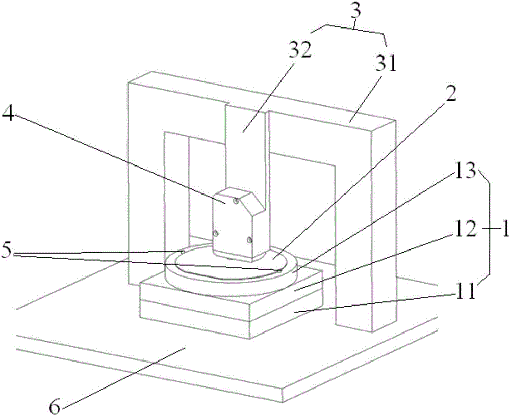
[0029] Such as figure 1 As shown, the present invention provides an optical waveguide wafer surface detection device, including a multi-directional motion platform 1 capable of moving in multiple directions along a horizontal plane, a laser confocal scanning probe 4 and a fixed bracket 3, the laser confocal scanning probe 4 is set on the fixed bracket 3, the wafer to be inspected 2 is placed on the multi-directional motion platform 1, and the laser confocal scanning probe 4 is located above the wafer to be inspected 2, the multi-directional The motion platform 1 drives the wafer to be inspected 2 to move in multiple directions, so that the laser confocal scanning probe 4 ...


PUM


Abstract

The invention relates to the technical field of wafer surface detection, and discloses a light waveguide wafer surface detecting device which comprises a multi-direction movement platform capable of moving in multiple directions of the horizontal plane, a laser confocal scanning measurement head and a fixed support.Due to the laser confocal scanning measurement head, by directly scanning a to-be-detected wafer, the warp rate and other data can be measured and the residual stress data of the surface of the wafer can be calculated, and ditches and other structural characteristics on the surface of the to-be-detected wafer can be directly obtained through scanning; the residual stress, ditches and other characteristics of the surface of the wafer can be detected at the same time and are prevented from being forwarded to different machines to be detected multiple times, the number of detection times of the surface of the wafer is greatly decreased, detection efficiency and precision are both high, and operation is convenient and rapid; in addition, due to the multi-direction movement platform, the to-be-detected wafer can be moved in multiple directions, the comprehensive scanning detection of the laser confocal scanning measurement head is greatly facilitated, the labor intensity of operators can be lowered, the time required by detection is shortened, and work efficiency is greatly improved.

Description

technical field [0001] The invention relates to the technical field of wafer surface detection, in particular to an optical waveguide wafer surface detection device. Background technique [0002] Optical fiber communication system is the core of today's information age. Various optical waveguide devices and optoelectronic devices are required in this system. The optical part of these devices usually has three structures, namely micro-optical structure, fiber optic structure and integrated optical structure. The integrated optical device in the integrated optical structure, also known as the optical waveguide device, refers to the optical waveguide device manufactured by the Planar Lightwave Circuit (PLC) process, which realizes light wave emission, detection, One or several functions such as coupling, beam splitting, wavelength division multiplexing and demultiplexing, filtering, and switching. Optical waveguide wafers are the front-end process products of optical waveguide...

Claims


Application Information

Patent Timeline
Patent Type & Authority Applications(China)
IPC IPC(8): H01L21/66H01L21/67
CPCH01L21/67288H01L22/10H01L22/12
Inventor 郑煜开小超夏冰心李白冰段吉安
Owner 黄山博蓝特半导体科技有限公司
Why Eureka
Try Eureka