Pixel circuit and driving method therefor, and organic light emitting display

A pixel circuit and organic technology, applied in the field of flat panel display, can solve the problems of uneven brightness of organic light-emitting displays, achieve the effects of improving display quality, avoiding threshold voltage deviation, and increasing service life

Active Publication Date: 2016-07-20
CHENGDU VISTAR OPTEOLECTRONICS CO LTD
View PDF3 Cites 28 Cited by
  • Summary
  • Abstract
  • Description
  • Claims
  • Application Information

AI Technical Summary

Problems solved by technology

[0006] The object of the present invention is to provide a pixel circuit and its driving method and an organic light emitting display to solve the problem of uneven brightness of the existing organic light emitting display

Method used


Image

  • Pixel circuit and driving method therefor, and organic light emitting display
  • Pixel circuit and driving method therefor, and organic light emitting display
  • Pixel circuit and driving method therefor, and organic light emitting display

Examples


Embodiment 1

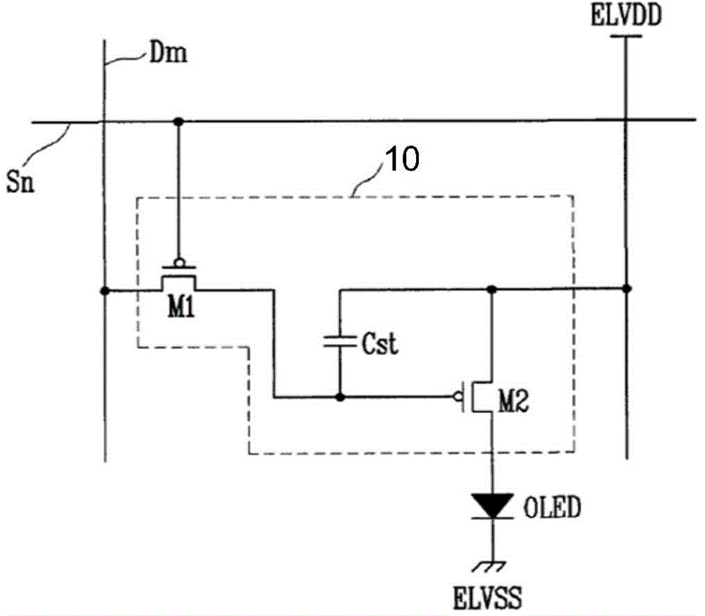
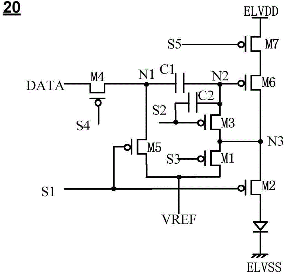
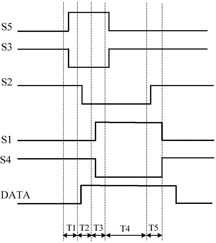
[0043] Please refer to figure 2 , which is a schematic structural diagram of a pixel circuit according to Embodiment 1 of the present invention. Such as figure 2 As shown, the pixel circuit 20 includes: a first thin film transistor M1 connected between the third node N3 and the third power supply VREF, and its gate connected to the third scanning line S3; a second thin film transistor M2 connected to the third power supply VREF; Between the three node N3 and the anode of the organic light emitting diode, its gate is connected to the first scanning line S1; the third thin film transistor M3 is connected between the second node N2 and the third node N3, and its gate is connected to the second The scan line S2; the fourth thin film transistor M4, connected between the data line DATA and the first node N1; the fifth thin film transistor M5, connected between the first node N1 and the third power supply VREF, whose gate is connected to the first Scanning line S1; the sixth thin...

Embodiment 2

[0083] Please refer to Figure 4 , which is a schematic structural diagram of a pixel circuit according to Embodiment 2 of the present invention. Such as Figure 4 As shown, the pixel circuit 30 includes: a first thin film transistor M1 connected between the third node N3 and the third power source VREF, and its gate connected to the third scanning line S3; a second thin film transistor M2 connected to the third power supply VREF; Between the three node N3 and the anode of the organic light emitting diode, its gate is connected to the first scanning line S1; the third thin film transistor M3 is connected between the second node N2 and the third node N3, and its gate is connected to the second The scan line S2; the fourth thin film transistor M4, connected between the data line DATA and the first node N1; the fifth thin film transistor M5, connected between the first node N1 and the third power supply VREF, whose gate is connected to the first Scanning line S1; the sixth thin...

Embodiment 3

[0088] Please refer to Image 6 , which is a schematic structural diagram of a pixel circuit according to Embodiment 3 of the present invention. Such as Image 6 As shown, the pixel circuit 40 includes: a first thin film transistor M1 connected between the third node N3 and the third power supply VREF, and its gate connected to the third scanning line S3; a second thin film transistor M2 connected to the third power supply VREF; Between the three node N3 and the anode of the organic light emitting diode, its gate is connected to the first scanning line S1; the third thin film transistor M3 is connected between the second node N2 and the third node N3, and its gate is connected to the second The scan line S2; the fourth thin film transistor M4, connected between the data line DATA and the first node N1; the fifth thin film transistor M5, connected between the first node N1 and the third power supply VREF, whose gate is connected to the first Scanning line S1; the sixth thin f...


PUM


Abstract

The invention provides a pixel circuit and a driving method therefor, and an organic light emitting display. The positive electrode of an organic light emitting diode is initialized by the pixel circuit through a first thin film transistor and a second thin film transistor; the gate electrode and the drain electrode of a sixth thin film transistor, taken as the driving element, are initialized through the first thin film transistor and a third thin film transistor; meanwhile, the overshoot current generated in the initializing process is eliminated through a seventh thin film transistor, so that the service life of the organic light emitting diode and the sixth thin film transistor is prolonged; and in addition, the current output by the sixth thin film transistor which is taken as the driving element is unrelated to the threshold value voltage of the sixth thin film transistor and the impedance of the power supply routing wires, so that uneven luminance caused by the threshold value voltage deviation of the thin film transistor and the difference of the impedance of the power supply routing wires can be avoided, and the display quality of the organic light emitting display is further improved.

Description

technical field [0001] The invention relates to the field of flat panel display technology, in particular to a pixel circuit, a driving method thereof, and an organic light-emitting display. Background technique [0002] Organic light-emitting display (English full name OrganicLightingEmittingDisplay, referred to as OLED) can emit light by itself, unlike thin film transistor liquid crystal display (English full name ThinFilmTransistorliquidcrystaldisplay, referred to as TFT-LCD) requires a backlight system (backlightsystem) to light up, so visibility and brightness are higher , and thinner. Currently, organic light-emitting displays are hailed as a new generation of displays that can replace thin-film transistor liquid crystal displays. [0003] Please refer to figure 1 , which is a circuit diagram of a pixel of an organic light emitting display in the prior art. Such as figure 1 As shown, each pixel of the organic light emitting display includes a pixel circuit 10 and a...

Claims


Application Information

Patent Timeline
Patent Type & Authority Applications(China)
IPC IPC(8): H01L27/32G09G3/32
Inventor 胡思明朱晖杨楠张婷婷刘周英
Owner CHENGDU VISTAR OPTEOLECTRONICS CO LTD
Why Eureka
Try Eureka