Supercharge Your Innovation With Domain-Expert AI Agents!

Spacer, spacer manufacturing method, mask and display device

A manufacturing method and spacer technology, which are applied in nonlinear optics, instruments, optics, etc., can solve problems such as poor thickness uniformity of liquid crystal cells, high contact surface pressure, and blurred display images, so as to improve display quality and increase Large area and better thickness uniformity

Active Publication Date: 2016-07-27
BOE TECH GRP CO LTD +1
View PDF6 Cites 12 Cited by
  • Summary
  • Abstract
  • Description
  • Claims
  • Application Information

AI Technical Summary

Problems solved by technology

During the production process of the above-mentioned PhotoSpacer, because the PhotoSpacer takes time to bake and shape, before the PhotoSpacer is formed, the edge of the PhotoSpacer will collapse under the influence of tension, so that the top surface of the finished PhotoSpacer is in the shape of a high center and a low circumference. When the photospacer is in the box, only the central part of the top surface of the PhotoSpacer is in contact with the array substrate or the color filter substrate, and the area of ​​the contact surface is small, which causes the pressure on the contact surface per unit area to become too large, and each PhotoSpacer is covered by the array substrate and color filter. The substrate is compressed and shortened, and the amount of shortening of each PhotoSpacer tends to become unbalanced, which makes the thickness uniformity of the liquid crystal cell between the array substrate and the color filter substrate worse, resulting in blurred display images

Method used


Image

  • Spacer, spacer manufacturing method, mask and display device
  • Spacer, spacer manufacturing method, mask and display device
  • Spacer, spacer manufacturing method, mask and display device

Examples


Embodiment Construction

[0031] In order to make the object, technical solution and advantages of the present invention clearer, the implementation manner of the present invention will be further described in detail below in conjunction with the accompanying drawings.

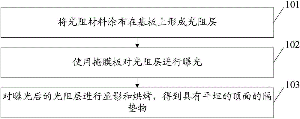
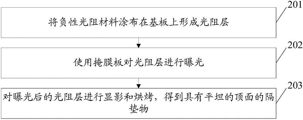
[0032] figure 1 It is a flow chart of a spacer manufacturing method provided by an embodiment of the present invention, see figure 1 , the method includes:

[0033] Step 101: Coating a photoresist material on a substrate to form a photoresist layer.

[0034] Step 102: exposing the photoresist layer using a mask.

[0035] Wherein, pattern area and non-pattern area are arranged on the mask plate; when the photoresist material is a negative photoresist material, the transmittance of the pattern area increases from the center to the edge; when the photoresist material is a positive photoresist material , the transmittance of the pattern area decreases from the center to the edge.

[0036] Wherein, the pattern area is used to form space...


PUM


Abstract

The invention belongs to the field of displays and discloses a spacer, a spacer manufacturing method, a mask and a display device. The method includes: coating a photoresist material on a substrate to form a photoresist layer; using the mask for exposure of the photoresist layer, wherein the mask is provided with a pattern area and a non-pattern area, and transmittance of the pattern area is progressively increased from center to edge if the photoresist material is a negative photoresist material and is progressively decreased from center to edge if the photoresist material is a positive photoresist material; subjecting the exposed photoresist layer to development and roasting to obtain the spacer with a flat top surface. Therefore, a contact surface area of the spacer is increased, mechanical strength is enhanced, thickness uniformity of a liquid crystal box between an array substrate and a color film substrate is optimized, and display quality is improved.

Description

technical field [0001] The invention relates to the field of displays, in particular to a spacer, a manufacturing method, a mask plate and a display device. Background technique [0002] Liquid crystal displays are widely used in various fields because of their advantages such as high image quality, low weight, low power consumption, and low radiation. The liquid crystal display panel is the most important component of the liquid crystal display. A liquid crystal display panel generally includes an array substrate, a color filter substrate disposed opposite to the array substrate, and liquid crystals filled between the array substrate and the color filter substrate. In order to ensure the thickness and uniformity of the liquid crystal cell, usually a plurality of spacers (PhotoSpacers) are arranged between the two substrates to isolate the space for injecting liquid crystals. [0003] The production process of the existing PhotoSpacer is as follows: the photoresist materia...

Claims


Application Information

Patent Timeline
Patent Type & Authority Applications(China)
IPC IPC(8): G02F1/1339
CPCG02F1/13394G02F1/13398
Inventor 冯彦贵熊正平李朝王静田利军
Owner BOE TECH GRP CO LTD
Features
  • R&D
  • Intellectual Property
  • Life Sciences
  • Materials
  • Tech Scout
  • Unparalleled Data Quality
  • Higher Quality Content
  • 60% Fewer Hallucinations
Learn More