Surface treatment method for compound semiconductor substrate and epitaxial structure

A surface treatment and semiconductor technology, applied in the field of surface treatment methods and epitaxial structures of compound semiconductor substrates, can solve problems such as cumbersome and complex treatment processes, increase surface roughness, simplify surface treatment processes, maintain high performance and high The effect of reliability

Active Publication Date: 2016-07-27
CHENGDU HIWAFER SEMICON CO LTD
View PDF3 Cites 2 Cited by
  • Summary
  • Abstract
  • Description
  • Claims
  • Application Information

AI Technical Summary

Problems solved by technology

[0004] However, most methods of patterning the substrate surface in the prior art are to process the substrate surface by photolithography or etching, and the processing technology is relatively complicated and cumbersome.

Method used


Image

  • Surface treatment method for compound semiconductor substrate and epitaxial structure
  • Surface treatment method for compound semiconductor substrate and epitaxial structure
  • Surface treatment method for compound semiconductor substrate and epitaxial structure

Examples


Embodiment Construction

[0021] The following will clearly and completely describe the technical solutions in the embodiments of the present invention with reference to the accompanying drawings in the embodiments of the present invention. Obviously, the described embodiments are only some, not all, embodiments of the present invention. Based on the embodiments of the present invention, all other embodiments obtained by persons of ordinary skill in the art without making creative efforts belong to the protection scope of the present invention.

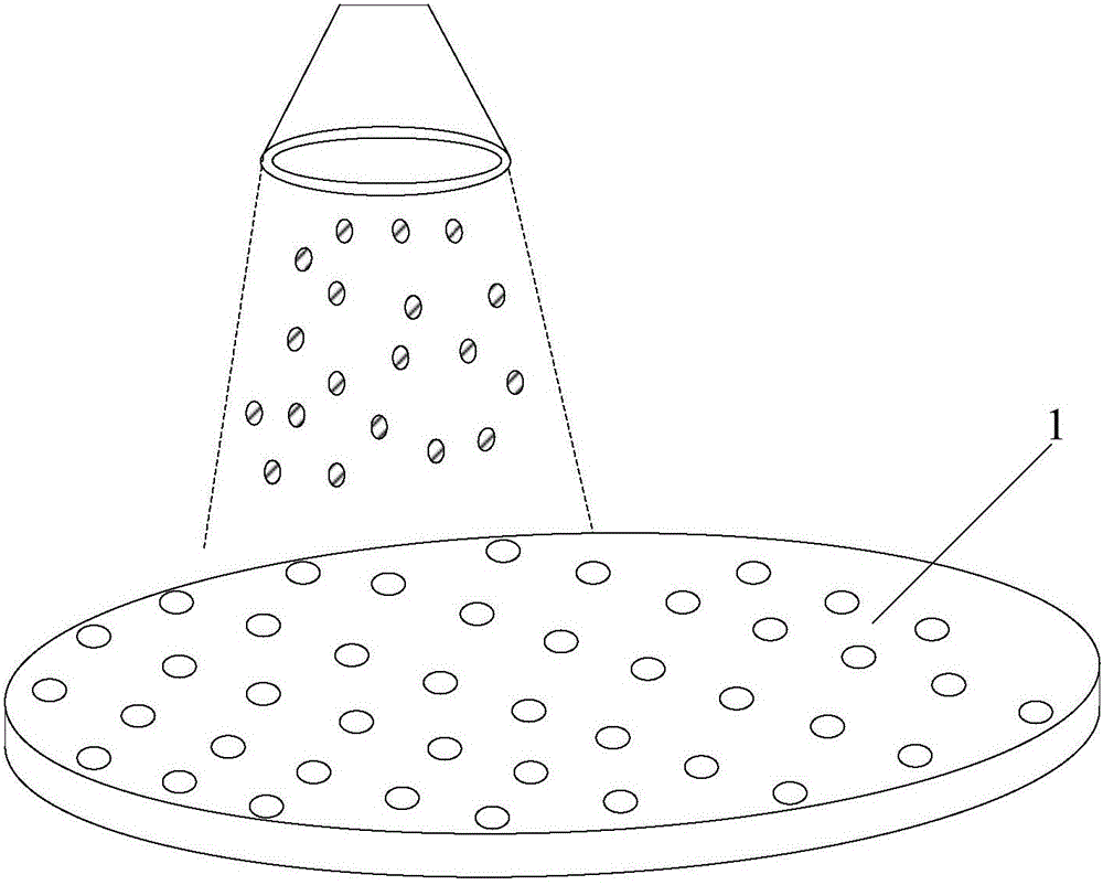
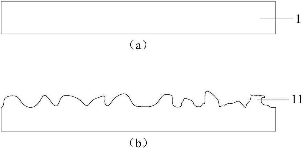
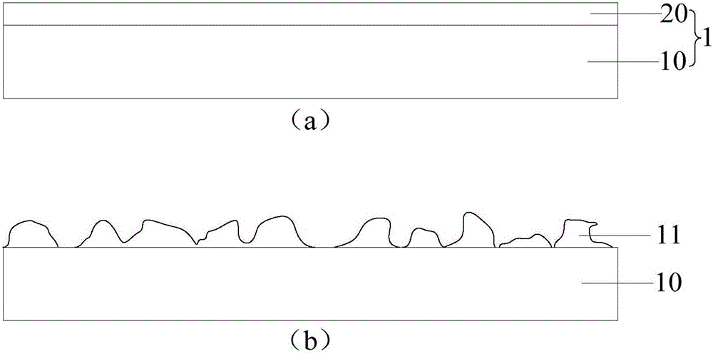
[0022] see figure 1 , is a schematic diagram of treating a compound semiconductor substrate with a surface treatment method for a compound semiconductor substrate according to an embodiment of the present invention. combined with the figure 1 The surface treatment method of the compound semiconductor substrate according to the embodiment of the present invention includes: high-pressure spraying a slurry containing abrasive toward the surface of the compound s...


PUM

PropertyMeasurementUnit
Diameteraaaaaaaaaa

Abstract

The invention provides a surface treatment method for a compound semiconductor substrate and an epitaxial structure. The surface treatment method comprises the following step of spraying slurry containing an abrasive material towards the surface of the compound semiconductor substrate at high pressure to form an irregular concave-convex structure on the surface of the compound semiconductor substrate. The epitaxial structure comprises the compound semiconductor substrate obtained by the surface treatment method and a compound semiconductor thin film; the compound semiconductor thin film transversely grows on the concave-convex structure of the compound semiconductor substrate; and the compound semiconductor substrate and the compound semiconductor thin film are in heterostructure. By the above method, the surface treatment technology can be simplified.

Description

technical field [0001] The invention relates to the technical field of semiconductor processing, in particular to a surface treatment method and an epitaxial structure of a compound semiconductor substrate. Background technique [0002] Compound semiconductor devices, especially the third-generation semiconductor devices represented by GaN and SiC, have broad application prospects in the fields of power electronics and communications. The performance and reliability requirements of the device are also very high. [0003] During the growth process of the compound semiconductor epitaxial structure, since the compound semiconductor material may need to be grown on a heterogeneous substrate, the lattice defect will be transmitted from the bottom to the top due to the lattice adaptation problem, which will affect the performance and reliability of the semiconductor device. In severe cases, it will cause device failure and damage. In order to overcome this defect, the lateral gr...

Claims


Application Information

Patent Timeline
IPC IPC(8): H01L21/304
CPCH01L21/3046
Inventor 李春江
Owner CHENGDU HIWAFER SEMICON CO LTD
Why Eureka
Try Eureka