3D NAND flash memory structure and manufacturing method

A manufacturing method and technology of flash memory, applied in semiconductor/solid-state device manufacturing, semiconductor devices, electrical components, etc., can solve problems such as chip failure, control gate failure, and easy introduction of defects, and achieve the effect of improving quality

Active Publication Date: 2016-07-27
GIGADEVICE SEMICON SHANGHAI INC +1
View PDF5 Cites 29 Cited by
  • Summary
  • Abstract
  • Description
  • Claims
  • Application Information

AI Technical Summary

Problems solved by technology

The existing method of removing excess tungsten on the sidewall is to use high-temperature mixed acid to directly remove excess tungsten on the sidewall and surface, which mainly has the following disadvantages: first, the reaction between the mixed acid and tungsten is slow, and the reaction time is long; secondly, The long-term wet process is easy to introduce defects, resulting in defective chips; in addition, in the actual production process, it is easy to cause unclean removal of tungsten on the side wall and surface, resulting in failure of the control gate

Method used


Image

  • 3D NAND flash memory structure and manufacturing method
  • 3D NAND flash memory structure and manufacturing method
  • 3D NAND flash memory structure and manufacturing method

Examples


Embodiment Construction

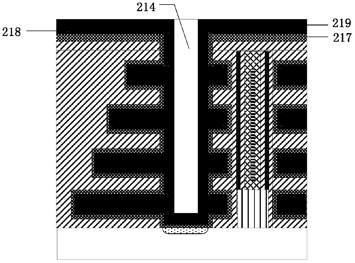
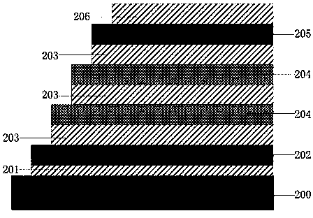
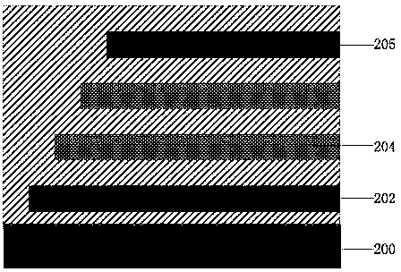
[0033] The present invention will be further described in detail below in conjunction with the accompanying drawings and embodiments. It should be understood that the specific embodiments described here are only used to explain the present invention, but not to limit the present invention. In addition, it should be noted that, for the convenience of description, only some structures related to the present invention are shown in the drawings but not all structures. It will be understood that although the terms first, second, etc. may be used herein to describe various elements, components, regions, layers and / or sections, these elements, components, regions, layers and / or sections should not be referred to by these Terminology restrictions. These terms are only used to distinguish one element, component, region, layer or section from another element, component, region, layer or section. Thus, a first element, component, region, layer or section discussed below could be termed...


PUM


Abstract

The invention discloses a 3D NAND flash memory structure and a manufacturing method. The method is characterized in that the method comprises the steps: providing a substrate, and forming a plurality of array string units, wherein the array string units are isolated through isolating trenches; each array string unit comprises polycrystalline silicon, a polycrystalline silicon dielectric layer, first material layers, and second material layers, wherein the first and second material layers are stacked together; the polycrystalline silicon dielectric layer is formed in the polycrystalline silicon; the second material layers are respectively formed between the adjacent first material layers; a wet etching method is used for removing the second material layers of the array string units, and a plurality of first recesses are formed; the inner walls of the isolating trenches and the inner walls of the first recesses are sequentially provided with grid blocking layers, adhesive layers and grid layers; the first recesses are filled with the grid layers; the method also comprises the steps: removing the grid layers through annealing treatment, and removing the grid layers outside the first recesses, and the adhesive layers, so as to effectively removing the grid layers of the side walls and the surface of a 3D NAND flash memory.

Description

technical field [0001] Embodiments of the present invention relate to memory manufacturing technologies, and in particular to a 3D NAND flash memory structure and manufacturing method. Background technique [0002] With the development of memory, the production process of semiconductors has made great progress. However, in recent years, the development of planar flash memory has encountered various challenges: physical limits, existing development technology limits, and storage electron density limits. In this context, in order to solve the difficulties encountered in planar flash memory and pursue lower production costs per unit storage unit, various three-dimensional (3D) flash memory structures have emerged, such as 3D NAND flash memory. [0003] In the 3D NAND process, tungsten gates are usually used as control gates. Unlike planar processes, 3D processes cannot remove the unnecessary tungsten gates by chemical mechanical polishing. The existing method of removing exce...

Claims


Application Information

Patent Timeline
Patent Type & Authority Applications(China)
IPC IPC(8): H01L21/8247H01L27/115
Inventor 许毅胜熊涛刘钊舒清明
Owner GIGADEVICE SEMICON SHANGHAI INC
Why Eureka
Try Eureka