Semiconductor device bonding structure and bonding method thereof

A bonding structure and semiconductor technology, applied in semiconductor devices, semiconductor/solid-state device manufacturing, semiconductor/solid-state device components, etc., can solve problems such as poor contact of pads, dishing, and reduced bonding performance, and achieve Accurate process is convenient, reduces the failure of electrical interconnection, and ensures the effect of bonding effect

Active Publication Date: 2018-11-27
GALAXYCORE SHANGHAI
View PDF6 Cites 0 Cited by
  • Summary
  • Abstract
  • Description
  • Claims
  • Application Information

AI Technical Summary

Problems solved by technology

[0003] The quality of the bonding is mainly determined by the flatness of the pad itself and the contact level between the pads. In the existing bonding process, the surface of the pad is prone to unevenness, which leads to poor contact between the pads, which makes different Poor connection between semiconductor devices, causing undesirable consequences such as circuit failure
[0004] Specifically, traditional bonding using the DBI method (Direct Bond Interconnect, DBI) completes the bonding by applying pressure and temperature between different metal pads (pads). In order to ensure the bonding effect, it is necessary to The flattening requirement is achieved through the CMP process, but due to the different selection ratio of the CMP slurry for copper and silicon dioxide, it will cause dishing on the top of the copper. If the two-layer interface passes through a metal pad with a depression Bonding, due to the unevenness of the interface, leads to a decrease in bonding performance, which is not good for bonding, and may lead to poor electrical connection of the entire circuit, thereby affecting the performance of the circuit

Method used


Image

  • Semiconductor device bonding structure and bonding method thereof
  • Semiconductor device bonding structure and bonding method thereof
  • Semiconductor device bonding structure and bonding method thereof

Examples


Embodiment Construction

[0035] In the following description, numerous specific details are set forth in order to provide a thorough understanding of the present invention. However, the present invention can be implemented in many other ways different from those described here, and those skilled in the art can make similar extensions without violating the connotation of the present invention, so the present invention is not limited by the specific embodiments disclosed below.

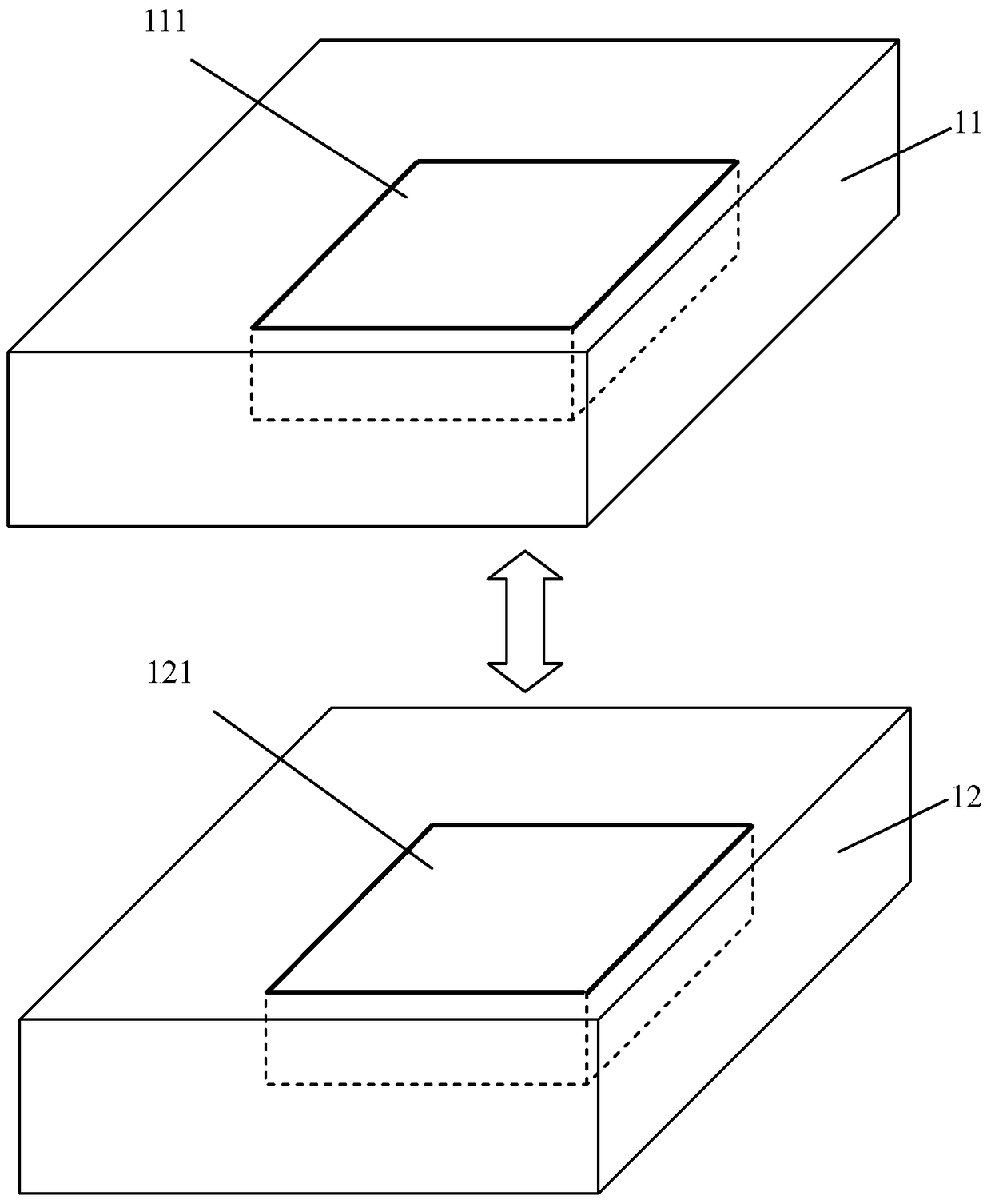
[0036] In the following, specific embodiments of the present invention will be described in conjunction with the accompanying drawings. refer to figure 1 As shown, it is a schematic diagram of the design of the pad in the prior art, wherein the first metal layer 11 and the second metal layer 12 are bonded, the first metal layer 11 includes the first pad 111, the second The metal layer 12 includes a second welding pad 121, wherein the bonding between the first welding pad 111 and the second welding pad 121 is a bonding using a...


PUM

PropertyMeasurementUnit
surface roughnessaaaaaaaaaa
angleaaaaaaaaaa

Abstract

The present invention relates to a semiconductor device bonding structure and a bonding method thereof. The bonding structure includes: a first metal layer, the surface of the first metal layer has a first pad, and the first pad has a first Opening pattern; second metal layer, the surface of the second metal layer has a second welding pad, and the second welding pad has a second opening pattern; the surface of the first metal layer and the second metal layer are bonded and connected , the first pad and the corresponding second pad are aligned up and down for bonding connection, the first opening pattern of the first pad and the second opening pattern of the second pad are mutually bonded on the bonding contact surface stagger.

Description

technical field [0001] The invention relates to the field of semiconductor device bonding, in particular to a semiconductor device bonding structure and a bonding method thereof. Background technique [0002] In the semiconductor circuit manufacturing process and in the later packaging process, different devices need to be bonded, and pads of different semiconductor devices are bonded to achieve the purpose of electrical connection. [0003] The quality of the bonding is mainly determined by the flatness of the pad itself and the contact level between the pads. In the existing bonding process, the surface of the pad is prone to unevenness, which leads to poor contact between the pads, which makes different The connection between semiconductor devices is not good, causing undesirable consequences such as circuit failure. [0004] Specifically, traditional bonding using the DBI method (Direct Bond Interconnect, DBI) completes the bonding by applying pressure and temperature b...

Claims


Application Information

Patent Timeline
Patent Type & Authority Patents(China)
IPC IPC(8): H01L23/485H01L23/488H01L21/60
CPCH01L24/05H01L24/08H01L24/80H01L2224/05552H01L2224/80895H01L2224/80896H01L24/09H01L2224/091H01L2224/80357H01L2224/08145H01L2924/00012
Inventor 赵立新
Owner GALAXYCORE SHANGHAI
Why Eureka
Try Eureka