

OLED device and preparing method thereof
A device and backplane technology, which is applied in the field of OLED devices and its preparation, can solve the problems of poor edge sealing, water vapor and oxygen penetration, etc.
- Summary
- Abstract
- Description
- Claims
- Application Information
AI Technical Summary
Problems solved by technology
Method used
Image

Examples
Embodiment Construction
[0023] The present invention will be described in detail below in conjunction with specific embodiments shown in the accompanying drawings. It is worth noting that the embodiments described below do not limit the present invention, and any structural, method, or functional changes made by those skilled in the art according to these embodiments are included in the protection scope of the present invention.
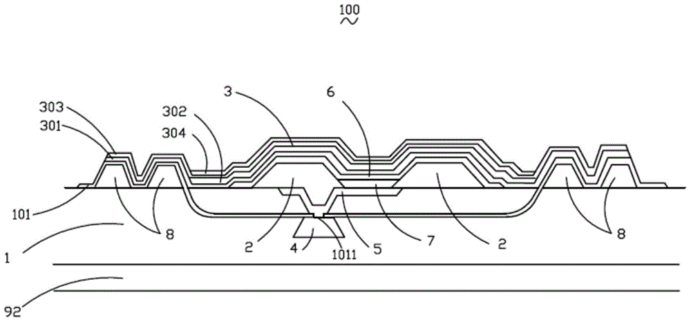
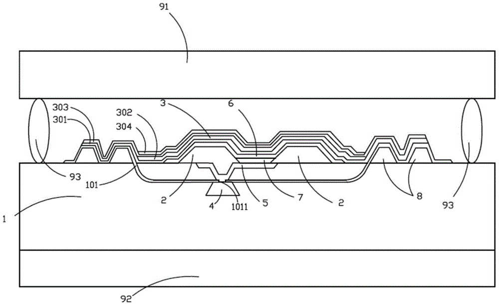
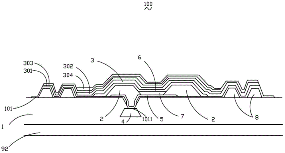
[0024] See Figure 1 to Figure 3 As shown, the OLED device 100 includes a TFT backplane 1 and a display unit located on the TFT backplane 1, and the display unit includes an anode layer 5, a cathode layer 6, and an OLED 7 located between the anode layer 5 and the cathode layer 6, The TFT backplane 1 is provided with a wall 8 surrounding the display unit; the TFT backplane 1 and the wall 8 are provided with an inorganic film 101; the display unit is located above the inorganic film 101 in the wall 8; The inorganic thin film 101 above the wall 8 and the display unit are depo...
PUM
 Abstract
Description
Claims
Application Information