A kind of mixed pin schottky diode and preparation method thereof

A technology of Schottky diode and conductivity type, which is applied in semiconductor/solid-state device manufacturing, semiconductor devices, electrical components, etc. It can solve the problems of high process complexity and difficulty in obtaining electrical indicators for GaNMPS devices, so as to avoid the problem of device performance Degradation, reducing the probability of impact ionization and avalanche breakdown, and avoiding the effect of excessive concentration of local electric field distribution

Inactive Publication Date: 2019-05-31
FUDAN UNIV +1
View PDF3 Cites 0 Cited by
  • Summary
  • Abstract
  • Description
  • Claims
  • Application Information

AI Technical Summary

Problems solved by technology

However, due to the large dislocation density between silicon and GaN and the high process complexity required to prepare a thin GaN drift region on a silicon substrate, it is difficult to obtain a good GaN MPS device based on this method. Electrical index

Method used


Image

  • A kind of mixed pin schottky diode and preparation method thereof
  • A kind of mixed pin schottky diode and preparation method thereof
  • A kind of mixed pin schottky diode and preparation method thereof

Examples


Embodiment Construction

[0042] In order to make the purpose, technical solutions and advantages of the present invention clearer, the technical solutions in the embodiments of the present invention will be clearly and completely described below in conjunction with the accompanying drawings in the embodiments of the present invention. It should be understood that the specific The examples are only used to explain the present invention, not to limit the present invention. The described embodiments are only some, not all, embodiments of the present invention. Based on the embodiments of the present invention, all other embodiments obtained by persons of ordinary skill in the art without making creative efforts belong to the protection scope of the present invention.

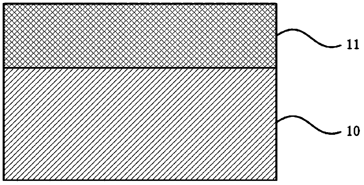
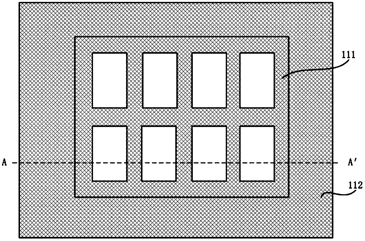
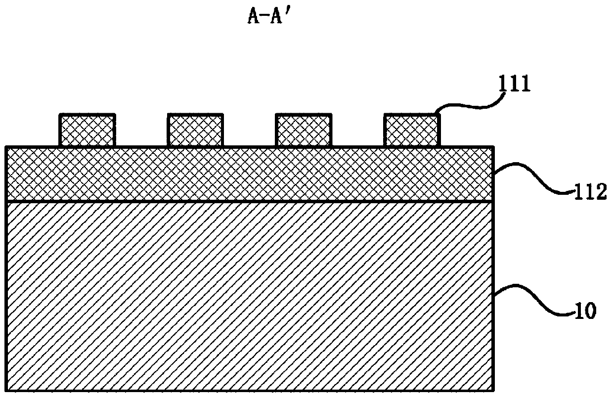
[0043] An embodiment of the hybrid PIN Schottky diode involved in the present invention will be described below with reference to the accompanying drawings. Such as Figure 9 As shown, the hybrid PIN Schottky diode includes: a GaN substr...


PUM

PropertyMeasurementUnit
thicknessaaaaaaaaaa
thicknessaaaaaaaaaa
depthaaaaaaaaaa

Abstract

The invention belongs to the technical field of semiconductor devices, and in particular relates to a hybrid PIN Schottky diode and a preparation method thereof. The hybrid PIN Schottky diode disclosed by the invention comprises a GaN substrate, a GaN epitaxial layer, a rectangular-ambulatory-plane GaN structure array, a double-edge terminal structure and a first metal structure, wherein the GaN epitaxial layer is formed on the GaN substrate; the rectangular-ambulatory-plane GaN structure array comprises a plurality of rectangular-ambulatory-plane GaN structures adjacent to each other and is formed on the GaN epitaxial layer; each rectangular-ambulatory-plane GaN structure comprises a GaN peripheral region and a GaN central region; the double-edge terminal structure is positioned on the periphery of the rectangular-ambulatory-plane GaN structure array and comprises a whole edge terminal compensation layer and a partial edge terminal compensation layer, wherein the whole edge terminal compensation layer is positioned on the partial edge terminal compensation layer; and the first metal structure is positioned on the rectangular-ambulatory-plane GaN structure array and is in Schottky contact with the GaN peripheral region. The relatively high reverse breakdown voltage can be obtained in the event that the area of a chip cannot be lost; simultaneously, the problem that the device performance is degraded due to the dislocation problem can be avoided; and thus, the hybrid PIN Schottky diode and the preparation method thereof disclosed by the invention can be well applied in the field of power electronics.

Description

technical field [0001] The invention belongs to the technical field of semiconductor devices, and in particular relates to a mixed PIN Schottky diode and a preparation method thereof. Background technique [0002] With the rapid development of information technology, high-power electronic devices such as power switches and power rectifiers have been widely used in various fields of national economy. As a substitute for traditional silicon-based power devices, power devices based on the third-generation wide-bandgap semiconductor GaN materials have attracted much attention because of their excellent material properties and device structure. GaN materials have a large bandgap and electron mobility. Good thermal stability and chemical stability, so it has a wide application prospect in the field of high power and high frequency, and has attracted attention and research. Today, breakthroughs have been made in GaN-based high electron mobility transistors, but the research on GaN...

Claims


Application Information

Patent Timeline
Patent Type & Authority Patents(China)
IPC IPC(8): H01L29/872H01L21/338
CPCH01L29/66143H01L29/872
Inventor 陈琳戴亚伟张宇李起鸣孙清清张卫
Owner FUDAN UNIV
Why Eureka
Try Eureka