Layout of sense amplifier and its forming method, layout of memory
A sensitive amplifier and graphic technology, applied in static memory, digital memory information, information storage, etc., can solve the problem of large area of the sensitive amplifier, achieve the effect of simplifying the method, realizing the circuit connection, and reducing the size
- Summary
- Abstract
- Description
- Claims
- Application Information
AI Technical Summary
Problems solved by technology
Method used
Image
Examples
Embodiment Construction
[0039] In order to make the above objects, features and advantages of the present invention more comprehensible, specific embodiments of the present invention will be described in detail below in conjunction with the accompanying drawings.
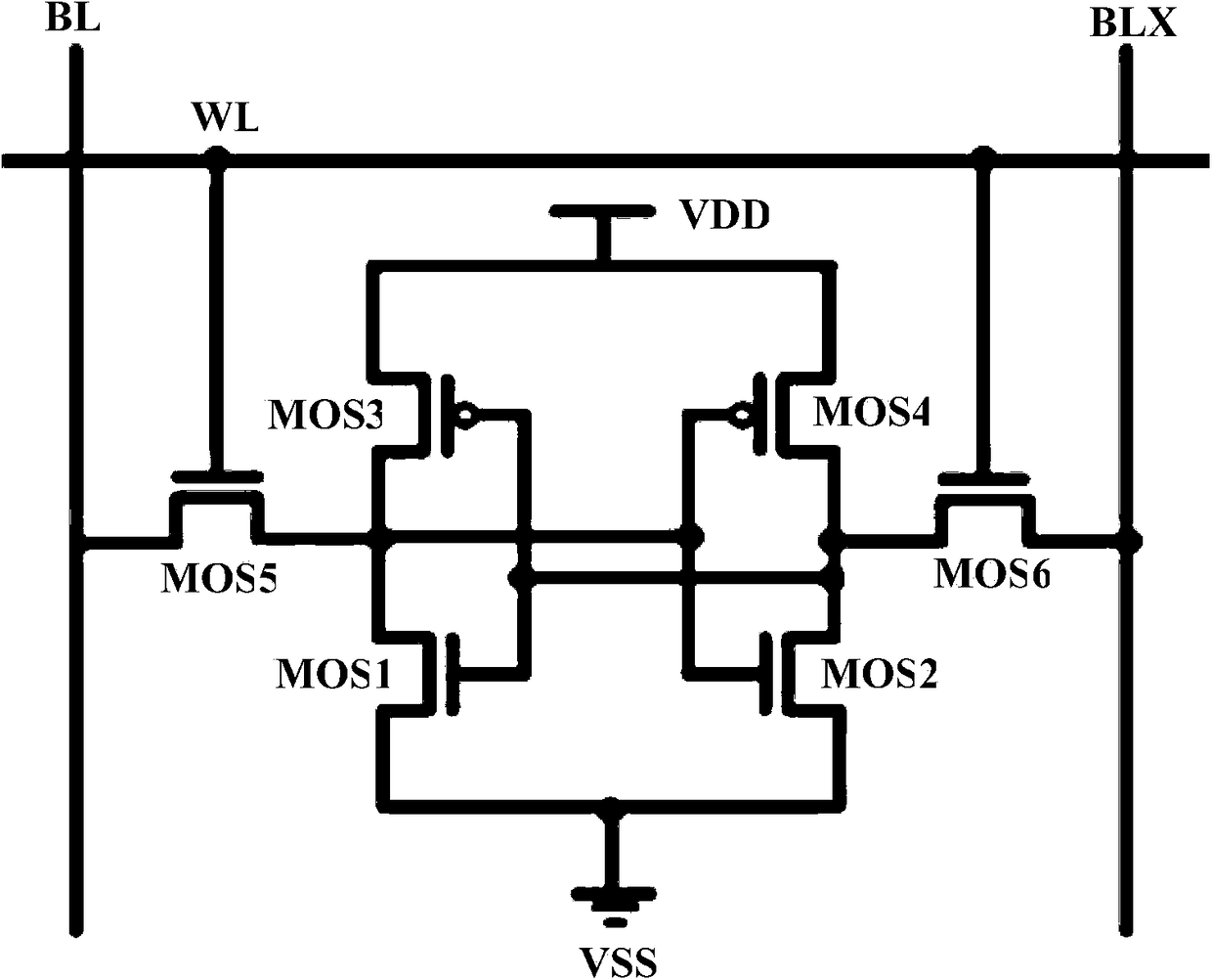
[0040] figure 1 It is a schematic diagram of a storage unit with an existing 6T structure. The storage unit includes: a first MOS transistor MOS1, a second MOS transistor MOS2, a third MOS transistor MOS3, a fourth MOS transistor MOS4, a fifth MOS transistor MOS5 and a sixth MOS transistor. MOS tube MOS6.
[0041] Both the source of the third MOS transistor MOS3 and the source of the fourth MOS transistor MOS4 are connected to the power line VDD. Both the source of the first MOS transistor MOS1 and the source of the second MOS transistor MOS2 are connected to the ground line VSS.
[0042] The drain of the third MOS transistor MOS3 is connected to the source of the fifth MOS transistor MOS5 , the drain of the first MOS transistor MOS1 , t...
PUM
 Abstract
Description
Claims
Application Information


