
FinFET (Fin Field Effect Transistor) and formation method thereof

A fin-type field effect and transistor technology, which is applied in semiconductor devices, semiconductor/solid-state device manufacturing, electrical components, etc., to achieve the effects of improving short channel effects, increasing channel area, and improving performance

Active Publication Date: 2016-08-03
SEMICON MFG INT (SHANGHAI) CORP
View PDF4 Cites 2 Cited by
  • Summary
  • Abstract
  • Description
  • Claims
  • Application Information

AI Technical Summary

Problems solved by technology

[0004] The performance of existing fin field effect transistors needs to be further improved

Method used


Image

  • FinFET (Fin Field Effect Transistor) and formation method thereof
  • FinFET (Fin Field Effect Transistor) and formation method thereof
  • FinFET (Fin Field Effect Transistor) and formation method thereof

Examples


Embodiment Construction

[0034] As mentioned in the background art, the performance of the existing FinFET needs to be further improved.

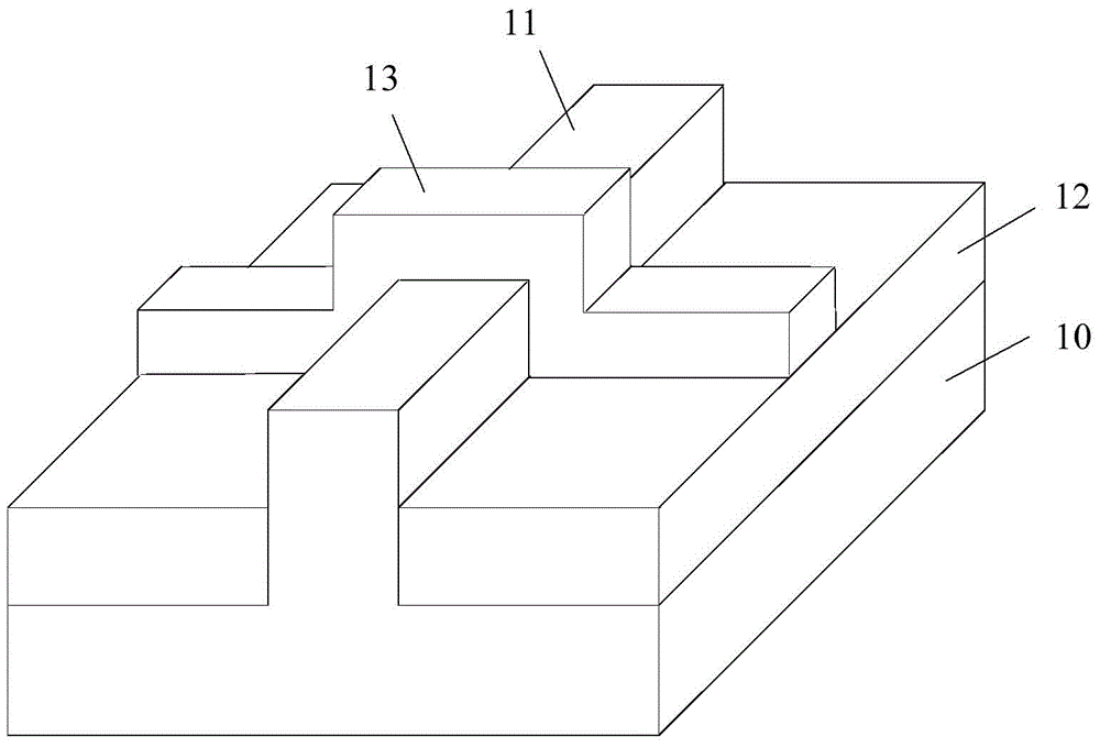
[0035] In an embodiment of the present invention, a fin having a first sub-fin and a second sub-fin is formed, the first sub-fin is located on the second sub-fin, and the width of the second sub-fin is smaller than that of the first sub-fin The width of the fin, and then form the gate structure across the fin, so that the channel area of ​​the transistor can be increased, thereby improving the performance of the fin field effect transistor.

[0036] In order to make the above objects, features and advantages of the present invention more comprehensible, specific embodiments of the present invention will be described in detail below in conjunction with the accompanying drawings.

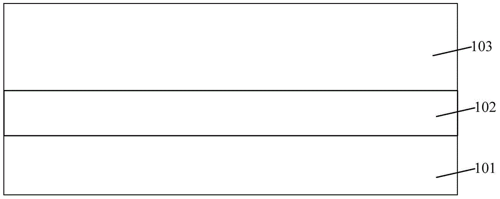
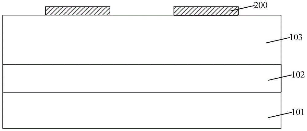
[0037] Please refer to figure 2 , providing a substrate, the substrate includes a first semiconductor layer 101 , an insulating layer 102 located on the surface of the first semiconductor ...


PUM

PropertyMeasurementUnit
Heightaaaaaaaaaa
Widthaaaaaaaaaa

Abstract

The invention relates to a FinFET (Fin Field Effect Transistor) and a formation method thereof. The formation method of the FinFET comprises the steps of providing a substrate, wherein the substrate comprises a first semiconductor layer, an insulating layer and a second semiconductor layer, forming a mask layer at partial surface of the second semiconductor layer and etching the second semiconductor layer by taking the mask layer as a mask to the insulating layer so as to form a fin portion, forming a sacrificial layer at the surface of the sacrificial layer, wherein the surface of the sacrificial layer is lower than top surface of the fin portion and covers partial side wall of the fin portion, and the part, which is higher than the sacrificial layer, of the fin portion acts as a first sub-fin portion, forming a protection layer at the side wall surface of the first sub-fin portion, removing the sacrificial layer, carrying out transverse etching on the fin portion along the exposed side wall of the fin portion so as to enable the width of partial fin portion to be reduced and enable the first sub-fin portion to be partially suspended, wherein the part, which is reduced in width, of the fin portion acts as a second sub-fin portion, and removing the protection layer and the mask layer and forming a gate structure which stretches across the first sub-fin portion and the second sub-fin portion. The formation method provided by the invention can improve the performance of the formed FinFET.

Description

technical field [0001] The invention relates to the technical field of semiconductors, in particular to a fin field effect transistor and a forming method thereof. Background technique [0002] With the continuous development of semiconductor process technology, process nodes are gradually reduced, and gate-last (gate-last) process has been widely used to obtain an ideal threshold voltage and improve device performance. However, when the feature size of the device is further reduced, even if the gate-last process is adopted, the structure of the conventional MOS field effect transistor can no longer meet the requirements for device performance, and the fin field effect transistor (FinFET) has been obtained as a multi-gate device. Widespread concern. The fin field effect transistor can effectively improve the short channel effect of the transistor and improve the performance of the device, and is widely used in semiconductor devices such as logic circuits and SRAM memories. ...

Claims


Application Information

Patent Timeline
IPC IPC(8): H01L21/336H01L29/78
Inventor 何有丰
Owner SEMICON MFG INT (SHANGHAI) CORP
Learn More