Automatic PCB optical detection method
An optical inspection and PCB board technology, applied in the field of optical inspection, can solve the problems of increased production and labor costs, batch scrap or repair, high labor costs, etc., and achieve the effects of reducing oxidation and fine dust, improving the quality of finished products, and improving work efficiency
- Summary
- Abstract
- Description
- Claims
- Application Information
AI Technical Summary
Problems solved by technology
Method used
Image

Examples
Embodiment 1
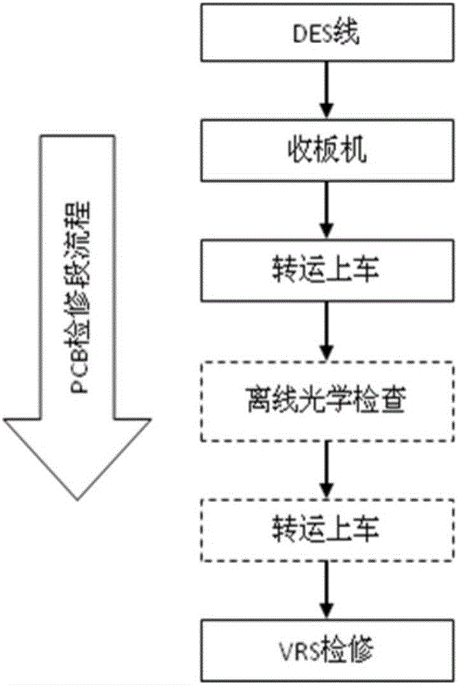
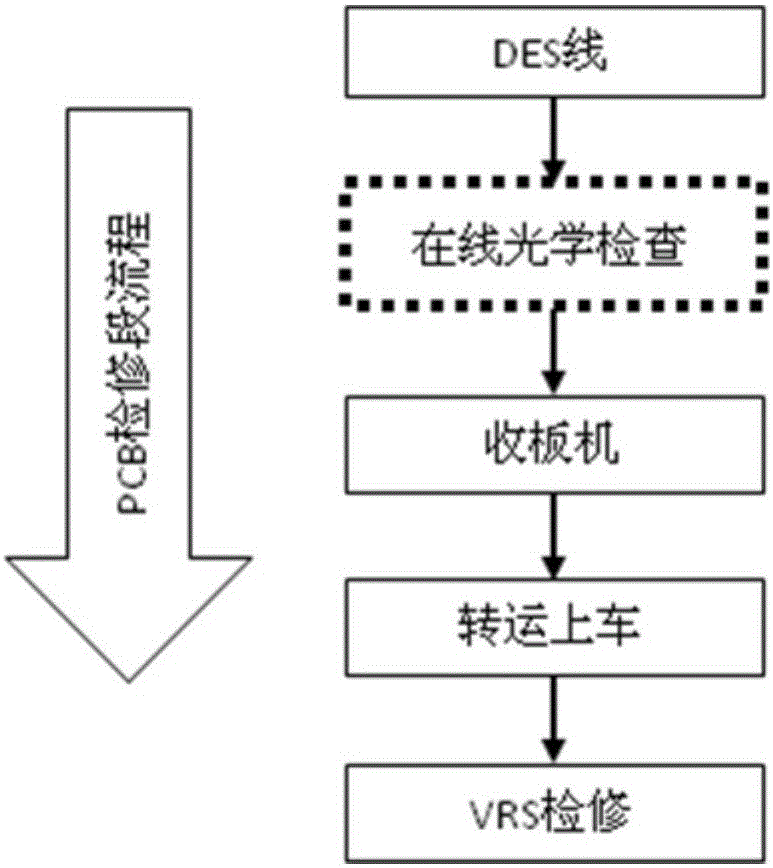
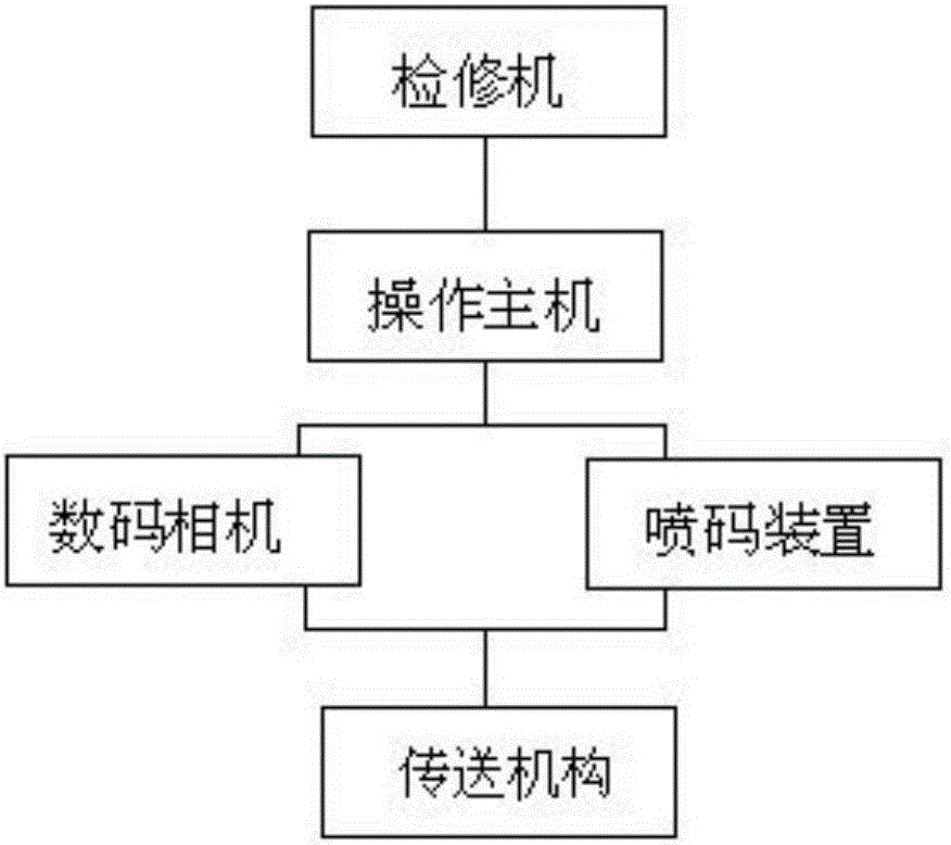
[0019] In this embodiment, online optical inspection equipment is set at the output end of the DES production line. The online optical inspection equipment includes a transmission mechanism, a digital camera, a coding device and an operating host. The transmission mechanism transmits the etched plate to the scanning area of the digital camera, and the etched plate There are digital cameras above and below the etched plate. When the etched plate is conveyed in the scanning area of the digital camera, the digital cameras above and below the etched plate simultaneously take pictures of the upper and lower surfaces of the etched plate. Compare and identify the grayscale mode and the original data, find out the abnormal points, and record each etched board as a unit; there is a coding device behind the scanning area of the digital camera. When the etched board is sent to the coding device, the coding device will The edge of the etched board is sprayed with codes, and at the sa...
Embodiment 2
[0025] The difference between this embodiment and Embodiment 1 is that the conveying speed of the etching plate in the digital camera scanning area is 4.8m / min, the angle of the etching plate in the digital camera scanning area is 3°, and the etching plate is in the digital camera scanning area. The transmission offset is 0.2cm, and the rest are basically the same as embodiment 1.
[0026] Integrated detection, accurate positioning of defects, timely feedback, shortened production time, avoided oxidation false spots, improved work efficiency, and improved product quality.
Embodiment 3
[0028] The difference between this embodiment and Embodiment 1 is that the transmission speed of the etched plate in the digital camera scanning area is 3.2m / min, the angle of the etched plate in the digital camera scanning area is 2°, and the etched plate is in the digital camera scanning area. The transmission offset is 0.8cm, and all the other are basically the same as embodiment 1.
[0029] Integrated detection, accurate positioning of defects, timely feedback, shortened production time, avoided oxidation false spots, improved work efficiency, and improved product quality.
PUM
 Abstract
Description
Claims
Application Information
 - Generate Ideas
- Intellectual Property
- Life Sciences
- Materials
- Tech Scout
- Unparalleled Data Quality
- Higher Quality Content
- 60% Fewer Hallucinations
Browse by: Latest US Patents, China's latest patents, Technical Efficacy Thesaurus, Application Domain, Technology Topic, Popular Technical Reports.
© 2025 PatSnap. All rights reserved.Legal|Privacy policy|Modern Slavery Act Transparency Statement|Sitemap|About US| Contact US: help@patsnap.com