Location method of failure point and failure analysis method of chip

A positioning method and a technology for positioning chips, which are applied in the direction of analyzing materials, using wave/particle radiation for material analysis, instruments, etc., can solve the problems of no solution, inability to determine the location of the failure point of the device, etc., and achieve the effect of reducing the impact

Active Publication Date: 2018-10-23
SEMICON MFG INT (SHANGHAI) CORP
View PDF7 Cites 0 Cited by
  • Summary
  • Abstract
  • Description
  • Claims
  • Application Information

AI Technical Summary

Problems solved by technology

However, with the reduction of device size (especially the size of 28nm / 32nm or below), the enhancement of density, and the complexity of device structure and doping process, the problem of accumulating charge on the sample surface will be amplified. As a result, more charges will accumulate on the sample surface after scanning (such as figure 1 As shown), it is impossible to effectively locate the location of the failure point
[0005] For example, in the potential contrast positioning method using a scanning electron microscope (SEM), since the surface charge cannot be conducted away, it will seriously affect the surface potential of the sample, and further affect the depth of the SEM image display, resulting in the inability to effectively locate location of failure
figure 2 Shown is the SEM image obtained by using the potential contrast positioning method provided in the prior art, from figure 2 It can be seen that there are multiple bright spots in the SEM image, so the location of the failure point in the device cannot be determined by the bright spots
For the above problems, there is currently no effective solution

Method used


Image

  • Location method of failure point and failure analysis method of chip
  • Location method of failure point and failure analysis method of chip
  • Location method of failure point and failure analysis method of chip

Examples


Embodiment 1

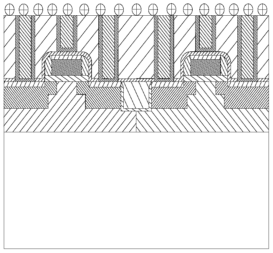
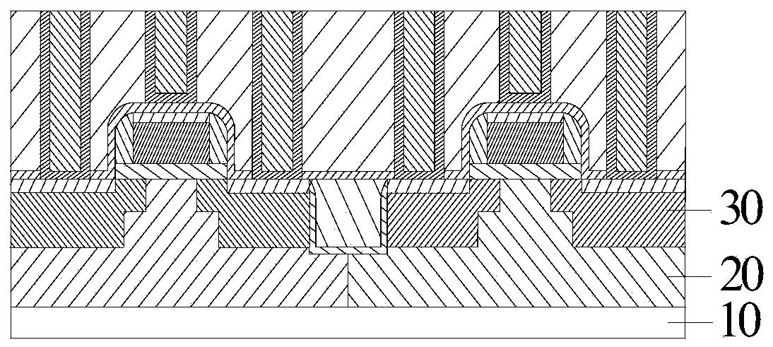
[0048] This embodiment provides a method for locating a failure point, including the following steps:

[0049] Firstly, the back of the chip is chemically mechanically polished so that the thickness of the substrate in the chip is 200nm; then, the back of the chemically mechanically polished chip is bombarded with an ion beam, the ion beam voltage is 150kV, and the bombardment particles are boron ions. The time is 10s, so that the ion beam passes through the devices in the chip; finally, the front side of the chip is peeled off to the surface to be tested, and then the front side of the chip is scanned by an electron beam with an accelerating voltage of 1kV in a scanning electron microscope to obtain a SEM. image, and use the lightness and darkness in the SEM image to determine the location of the failure point in the chip.

Embodiment 2

[0051] This embodiment provides a method for locating a failure point, including the following steps:

[0052] First, the back of the chip is chemically mechanically polished so that the thickness of the substrate in the chip is 300nm; after that, the back of the chip is subjected to vibration treatment with ultrasonic waves, and the time of the vibration treatment is 60s; Rinse the back of the chip, and use an air gun to dry the back of the rinsed chip; then, bombard the back of the chemically mechanically polished chip with an ion beam, the ion beam voltage is 200kV, and the bombarded particles are phosphorus ions. The bombardment time is 60s, so that the ion beam passes through the devices in the chip; finally, the front side of the chip is peeled off to the surface to be tested, and then the front side of the chip is scanned by an electron beam with an accelerating voltage of 1.5kV in the scanning electron microscope to A SEM image is obtained, and the position of the fail...

Embodiment 3

[0054] This embodiment provides a method for locating a failure point, including the following steps:

[0055] First, the back of the chip is chemically mechanically polished so that the thickness of the substrate in the chip is 310nm; then, the back of the chip is subjected to vibration treatment with ultrasonic waves, and the time of the vibration treatment is 300s, and then deionized water is used to deionize the substrate after the vibration treatment. Rinse the back of the chip, and use an air gun to dry the back of the rinsed chip; then, bombard the back of the chemically mechanically polished chip with an ion beam, the ion beam voltage is 210kV, and the bombardment particles are argon atoms. The bombardment time is 65s, so that the ion beam passes through the devices in the chip; finally, the front side of the chip is peeled off to the surface to be tested, and then the front side of the chip is scanned by an electron beam with an accelerating voltage of 2kV in the scann...


PUM

PropertyMeasurementUnit
thicknessaaaaaaaaaa

Abstract

The invention provides a failure point positioning method and a chip failure analysis method. Specifically, a chip comprises a substrate and a device located at the substrate. The positioning method includes: conducting thinning treatment on the back of the chip to a state close to the device; carrying out ion beam bombardment on the back of the chip subjected to thinning treatment so as to make an ion beam pass through the device; and performing electron-beam scanning on the front of the chip subjected to ion beam bombardment so as to position the location of a failure point in the chip. By means of ion beam bombardment on the back of the chip subjected to thinning treatment, the method provided by the invention makes the ion beam pass through the device and generates a breakdown area in the device, so that when a to-be-detected surface of the chip is scanned by electron beam, the surface charge generated on the to-be-detected surface can be released along the breakdown area on the device surface, the influence of surface charge on the device surface potential can be reduced, and then the position of the failure point in the device can be acquired accurately.

Description

technical field [0001] The present application relates to the technical field of semiconductor integrated circuits, in particular, to a method for locating a failure point and a method for analyzing failure of a chip. Background technique [0002] For chip failure analysis, the location of the failure point is very critical. Generally, the specific location of the failure point in the chip is determined by determining the failure point, so as to analyze the failure mechanism of the chip. Among the failure point location methods, the potential contrast location method is a widely used precise location method, which uses an electron beam to scan the surface of the sample to be tested to obtain the location of the failure point. [0003] In the prior art, the steps of the potential contrast positioning method using a scanning electron microscope (SEM) are: first, the sample is processed to the current layer to be observed; Measurement surface) to scan; Finally, the location of...

Claims


Application Information

Patent Timeline
Patent Type & Authority Patents(China)
IPC IPC(8): G01N23/2251G01N23/2202
Inventor 殷原梓
Owner SEMICON MFG INT (SHANGHAI) CORP
Why Eureka
Try Eureka