SICM amplitude modulation imaging mode scanning device and method

An imaging mode and amplitude modulation technology, applied in measurement devices, scanning probe technology, scanning probe microscopy, etc., can solve problems such as dependence, and achieve the effects of low cost, accelerated scanning, and high sensitivity

Inactive Publication Date: 2016-08-10
SHENYANG INST OF AUTOMATION - CHINESE ACAD OF SCI
View PDF5 Cites 6 Cited by
  • Summary
  • Abstract
  • Description
  • Claims
  • Application Information

AI Technical Summary

Problems solved by technology

However, the phase modulation mode must detect the current signal in phase with the driving voltage, so it must rely on the lock-in amplifier, which is a relatively expensive instrument

Method used


Image

  • SICM amplitude modulation imaging mode scanning device and method
  • SICM amplitude modulation imaging mode scanning device and method
  • SICM amplitude modulation imaging mode scanning device and method

Examples


Embodiment 1

[0051] 1. Use a silicon material standard grid (P / N 498-000-026, Digital Instruments, Inc.) with a width of 5 μm and a depth of 200 nm as a master mold, and pour 10:1 PDMS (Sylgard 184, Dow Corning) main ingredient and hardener are stirred evenly; then vacuumize for 20 minutes to make the mixture free of bubbles; then place it on a heating plate (PC-600, Corning) and bake at 70°C for 4-5 hours; Finally, the cured PDMS layer is torn off from the silicon material standard grid. At this time, the PDMS surface close to the silicon grid will be imprinted with a fine structure complementary to the grid, so that the PDMS material grid sample is obtained.

[0052] 2. Place the PDMS sample with the imprinted structure facing up, dip the bottom surface in a Φ35mm petri dish, use a micropipette to inject phosphate buffered saline (PBS) into the petri dish, and the liquid level is 2mm above the surface of the PDMS sample is the best;

[0053] 3. The glass tube probe is drawn by a borosili...


PUM


Abstract

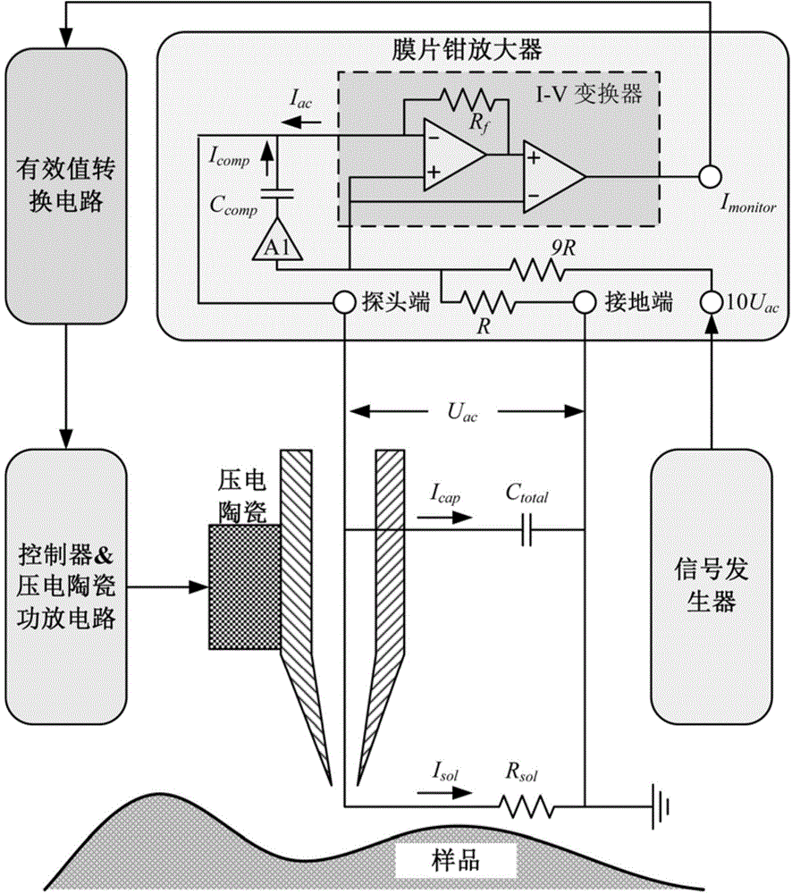
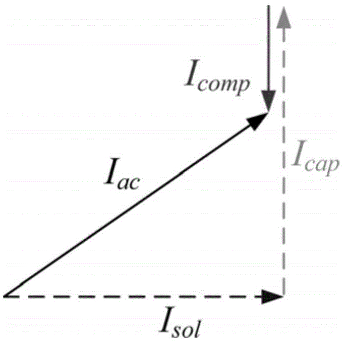
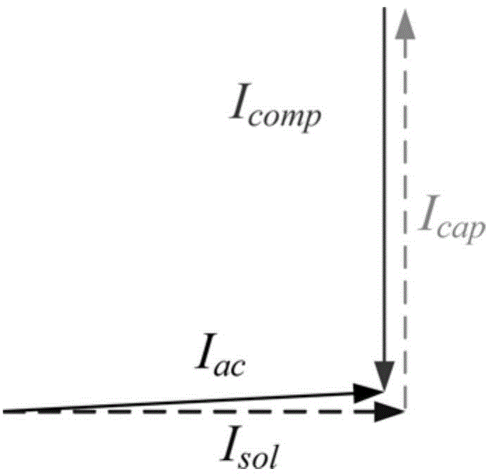
The invention relates to an SICM (Scanning Ion Conductance Microscope) amplitude modulation imaging mode scanning device, comprising a signal generator, a patch clamp amplifier, an effective value conversion circuit, a controller, a probe, an XY nano platform, and a Z-direction nano piezoelectric ceramic element, wherein the signal generator, the patch clamp amplifier, the effective value conversion circuit and the controller are connected in sequence. A method provided by the invention comprises the following steps: the signal generator outputs an alternating current signal to the patch clamp amplifier; the compensation capacitance of the patch clamp amplifier is adjusted; and the effective value conversion circuit calculates the effective value of current amplitude, and feeds the effective value of amplitude back to the controller, and the controller controls the height of the probe in real time according to the effective value of amplitude to realize sample scanning. According to the invention, the alternating current amplitude is used as a feedback value, so the defects of a direct-current mode such as direct-current drift and vulnerability to electrical noise are overcome. Higher modulation frequency is achieved compared with the traditional alternating-current mode, and scanning is accelerated.

Description

technical field [0001] The invention relates to a low-cost, fast and high-stability non-destructive imaging technology, in particular to a scanning device and method of a novel imaging mode amplitude modulation mode based on scanning ion conductance microscope (SICM) technology. Background technique [0002] Scanning ion conductance microscope (SICM) is a member of the scanning probe microscope family. By detecting the ion current flowing through the ultrafine glass tube probe, it can realize non-contact force scanning on the surface of the sample, and then study the sample. shape and properties. SICM has the characteristics of non-contact nondestructive scanning, high imaging resolution, and easy preparation of probes, and is especially suitable for studying living cells under physiological conditions. At present, research groups have conducted nanoscale morphology observations on living biological samples such as cardiomyocytes, renal epithelial cells, and nerve cells. ...

Claims


Application Information

Patent Timeline
Patent Type & Authority Applications(China)
IPC IPC(8): G01Q60/44
Inventor 刘连庆李鹏李广勇王越超杨洋周磊王栋
Owner SHENYANG INST OF AUTOMATION - CHINESE ACAD OF SCI
Why Eureka
Try Eureka