Transparent Conducting Components and Related Electro-Optic Modulator Devices

a transparent conducting component and modulator technology, applied in optics, instruments, nanotechnology, etc., can solve the problems of limited low-voltage operation of prior high-speed electro-optic device structures, limited metal absorption, and limited metal electrode closeness, etc., to achieve high modulation speed, not limited, and high eo coefficient

Active Publication Date: 2011-03-10
NORTHWESTERN UNIV
View PDF5 Cites 4 Cited by
  • Summary
  • Abstract
  • Description
  • Claims
  • Application Information

AI Technical Summary

Benefits of technology

[0007]It is an object of this invention to provide an electro-optic modulator device, in comparison to the prior art, with lower switching or modulation voltages achievable without incurring higher optical losses. Alternatively, it is a related object to provide such devices with switching or modulation voltages comparable to the prior art, but achievable with smaller device sizes.
[0019]Accordingly, this invention can meet one or more of the objectives provided or inferred from the preceding, and can be directed to optical intensity / phase modulation and, more specifically, to the design of modulator device structures that can (1) reduce the driving voltage of a polymer EO modulator, (2) without increasing device length, while (3) significantly lowering high modulation frequency.

Problems solved by technology

For a given electro-optically active material, the prior high-speed electro-optic device structures are limited in their ability to provide low voltage operation.
Metals, however, are very absorptive with respect to an optical beam propagating within the electro-optically active material.
This limits how close the metal electrodes can be, which subsequently limits the strength of the electric field achievable at the electro-optically active material and, hence, the modulator voltage.
The present electro-optic modulator structures are thus incapable of achieving much lower modulation voltages without incurring higher optical losses.
Such considerations make it difficult to achieve low modulation voltage, high integration density, or smaller device sizes, and consequently limit applications of such devices

Method used


Image

  • Transparent Conducting Components and Related Electro-Optic Modulator Devices
  • Transparent Conducting Components and Related Electro-Optic Modulator Devices
  • Transparent Conducting Components and Related Electro-Optic Modulator Devices

Examples


example 1

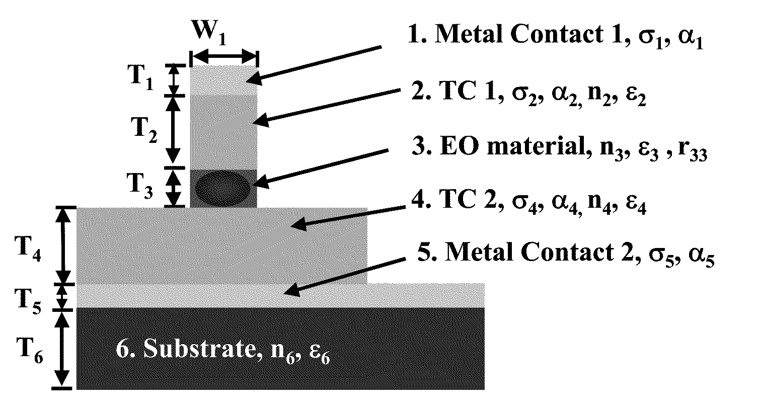
[0062]For a device structure of such embodiments, the waveguide core layer can be any EO material, such as a poled polymer, self-assembled polymer, LiNbO3, BaTiO3, a semiconductor (e.g., GaAs, AlAs, AlGaAs, InP, InGaAs, InGaAsP) or others. PEPCOOH (e.g., a self-assembled polymer; that is, Pyridine-Ethene-Pyrrole-Carboxylic Acid) is used as an example (refractive index n=1.9 at 1.55 μM wavelength). The TC cladding can be any known TC or TCO, such as but not limited to the polymeric materials described herein, as well as ZnO, ZIO, GIO, GITO, ZITO, ITO, CdO or others. Here, ZITO can be used for purpose of example (refractive index n=1.7 at 1.55 μM wavelength). For a device structure, the ridge etching can stop anywhere from the top TCO to the bottom metal, which will give a different mode size of waveguide, single mode or multi mode. Three examples are presented: a 1st example with etching to the bottom TCO after the EO material, a 2nd example with etching to the bottom metal, and a 3r...

example 1a

1st Example with Etching to Bottom of TCO after EO Material

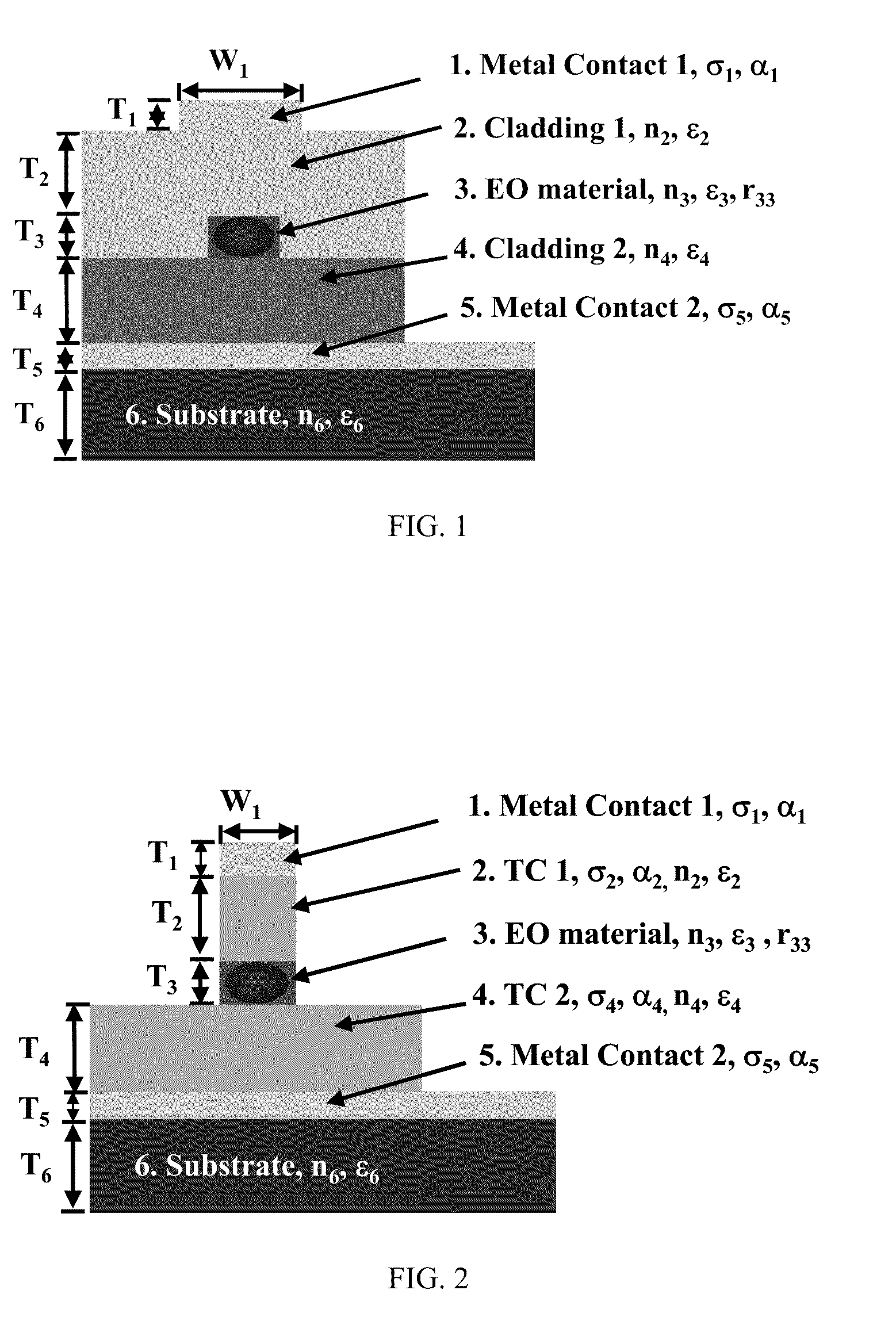
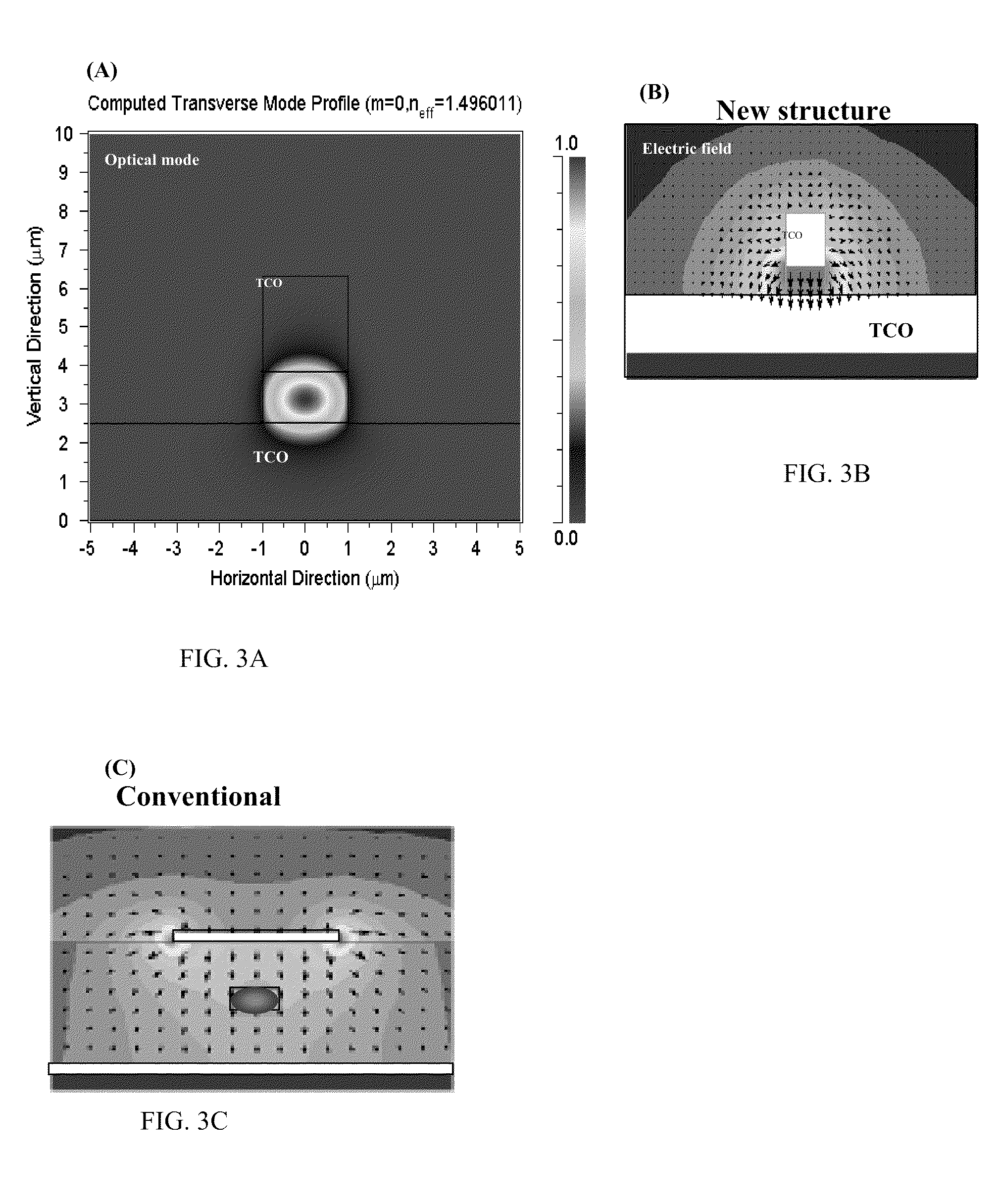
[0063]With reference to the device structure shown in FIG. 2, a TCO thickness is 2 μM (e.g., thick enough to reduce metal loss αL<0.3d) and core layer is 1 μM; waveguide width is 2 μM. As shown in FIG. 3, simulation results clearly show good optical confinement and much stronger electric field (FIG. 3B) cross the EO material compared to a conventional structure (FIG. 3C).

[0064]A planar structure as the bottom TCO instead of a ridge structure will give a smaller resistance due to the larger area, ˜2× different (R top=2.19R bottom for this example). The top and bottom TCO can be single layer or multi-layer with the same or different electric conductivity.

[0065]To illustrate a single layer TC electrode, a waveguide core layer is PEPCOOH with an EO coefficient r33=120 pm / V and a refractive index n=1.9. The cladding layer is ZITO with a refractive index n=1.7. With three refractive indices, the core thickness and cladding thickne...

example 1b

2nd Example with Etching to Bottom Metal after TCO

[0074]Another device structure is shown in FIG. 4. With this structure, optical confinement is stronger than that available using the structure of Example 1a. The waveguide can be narrower for nano-scale application. TC parameter calculations for a target Vπ and frequency responses are based on the principles discussed in Example 1a.


PUM

PropertyMeasurementUnit
frequenciesaaaaaaaaaa
modulation voltageaaaaaaaaaa
switching voltagesaaaaaaaaaa

Abstract

New electro-optic (EO) phase modulator devices and geometries, as can be constructed using a transparent conductive component.

Description

[0001]This application is a continuation of and claims priority benefit from application Ser. No. 11 / 888,503 filed Aug. 1, 2007 and now issued as U.S. Pat. No. 7,835,597 on Nov. 16, 2010, which is a continuation-in-part of and claims priority benefit from co-pending application Ser. No. 11 / 225,553 filed Sep. 13, 2005 which claims priority from prior provisional application Ser. No. 60 / 609,433, filed Sep. 13, 2004 and prior provisional application Ser. No. 60 / 704,644, filed Aug. 2, 2005, and claims priority benefit from prior provisional application 60 / 834,593, filed Aug. 1, 2006, each of which is incorporated herein by reference in its entirety.[0002]This invention was made with government support under Grant No. DAAD-19-00-1-0368 awarded by the Army Research Office and Grant No. DMR-00769097 awarded by the National Science Foundation. The government has certain rights in the invention.FIELD OF THE INVENTION[0003]This invention relates to electro-optic modulators, modulator geometri...

Claims


Application Information

Patent Timeline
Patent Type & Authority Applications(United States)
IPC IPC(8): G02F1/035
CPCB82Y20/00G02F1/0018G02F1/035G02F1/0316G02F1/017
Inventor MARKS, TOBIN J.HO, SENG-TIONGMA, JINGXU, GUOYANG
Owner NORTHWESTERN UNIV
Why Eureka
Try Eureka