Capacitive flexible pressure sensor based on microstructural dielectric layers and preparation method of capacitive flexible pressure sensor

A pressure sensor and micro-structured technology, applied in the field of sensors, can solve the problem that the sensitivity and stability of the sensor need to be further improved, and achieve the effects of being conducive to application promotion, low energy consumption and low cost

Active Publication Date: 2016-08-17
XIAMEN ZHONGKE WISDOW MEDICAL TECH CO LTD
7 Cites 94 Cited by

AI-Extracted Technical Summary

Problems solved by technology

The disadvantage of this technical solution is that the sensitivity and stability of the sensor need to be further improved
[0005] However, the theoretical and experimental methods o...

Method used

The present invention is by designing and making the dielectric layer of different microstructures, reaches the purpose of adjusting the rate of change of the distance between two conductive layers and the air occupancy rate in the stress process, thereby effectively adjusting the sensitivity and test range of the flexible pressure sensor, etc. performance.
The present invention overcomes many difficulties, has prepared the capacitive flexible pressure sensor based on the mi...

Abstract

The invention relates to a capacitive flexible pressure sensor based on microstructural dielectric layers and a preparation method of the capacitive flexible pressure sensor and belongs to the technical field of sensors. The capacitive flexible pressure sensor comprises an upper flexible substrate, a lower flexible substrate, an upper conducting layer and a lower conducting layer, wherein the upper conducting layer is attached to the inner surface of the upper flexible substrate, the lower conducting layer is attached to the inner surface of the lower flexible substrate, and the microstructural dielectric layers are arranged between the upper conducting layer and the lower conducting layer. Compared with the prior art, different microstructural dielectric layers are designed for the capacitive flexible pressure sensor, the sensor performance can be effectively regulated according to change of conditions such as shape, size, distribution and the like of each dielectric layer microstructure, and preparation of the capacitive flexible pressure sensors with different sensitivity and test ranges is realized. Besides, the microstructures prepared with methods such as microcapsule foaming, impressing, replica transfer, 3D printing and the like are low in cost, high in efficiency, low in energy consumption and particularly suitable for large-area and large-scale production, and application and popularization of the sensor are facilitated.

Application Domain

Force measurementFluid pressure measurement using capacitance variation

Technology Topic

Image

  • Capacitive flexible pressure sensor based on microstructural dielectric layers and preparation method of capacitive flexible pressure sensor
  • Capacitive flexible pressure sensor based on microstructural dielectric layers and preparation method of capacitive flexible pressure sensor
  • Capacitive flexible pressure sensor based on microstructural dielectric layers and preparation method of capacitive flexible pressure sensor

Examples

  • Experimental program(3)

Example Embodiment

[0064] Example 1:
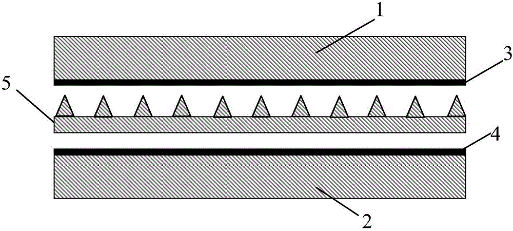
[0065] (1) Preparation of flexible substrate
[0066] The commercially available PDMS monomer and curing agent (Dow Corning, SYLGARD 184, USA) are thoroughly mixed according to a mass ratio of 10:1, using OSP-100 Meyer rod (OSP-100, Shijiazhuang OSP Machinery Technology Co., Ltd. ) Coat on the surface of commercially available inkjet printing photo paper (Canon, LU-101 Professional Suede Photo Paper, Japan), then place it in a vacuum oven at room temperature for 5 minutes to remove air bubbles in the coating, and then cure at 70°C 2 It was peeled off the surface of the photographic paper to obtain a flexible substrate with a thickness of 100 μm.
[0067] (2) Preparation of conductive layer and electrode
[0068] Using screen printing method (screen printing machine: OS-500FB, China Ou Laite Printing Machinery Industry Co., Ltd.), printed nano silver conductive ink (AP02, Beijing Beiyin Zhongyuan Technology Co., Ltd.) on the surface of the flexible substrate to obtain the conductive layer , The surface resistance is 10Ω/sq. Silver conductive glue (Ablestik, Ablebond 84-1Limisr4) is used to form upper and lower conductive electrodes on the two conductive layers, and copper wires are drawn from the conductive layers for sensor performance testing.
[0069] (3) Preparation of foamed microcapsules
[0070] a. Dissolve 1.75g ​​of phenolic epoxy resin (F51, Bluestar New Chemical Materials Co., Ltd. Wuxi Resin Factory) at 60°C in 10ml of trimethylethylsilane (chemically pure, Beijing Chemical Factory) solvent to obtain solution A spare;
[0071] b. Dissolve 3g of gum arabic (chemically pure, Xilong Chemical Factory, Shantou, Guangdong) in 150ml of water to obtain B solution for use;
[0072] c. Add the A solution prepared in the above steps to the B solution, stir and emulsify at 60°C for 3 hours at a speed of 400 rpm to obtain a stable emulsion system (electric mixer D2004W, Hesler Instrument Co., Ltd.);
[0073] d. Dissolve 0.72g of polyamide curing agent (YF-650, Guangzhou Yihuisheng Chemical Co., Ltd.) in 50ml of water, and add it to the emulsion formed in step c to react for 1 hour to obtain a foamed microcapsule dispersion; The foamed microcapsule dispersion is filtered through filter paper and dried in an oven at 60°C for 1 hour to obtain foamed microcapsule powder; diagram 2-1 As shown, the optical microscope picture of the foamed microcapsule powder of this example, such as Figure 2-2 As shown, the SEM image of the single foamed microcapsules of this example has an average particle size of about 5 μm.
[0074] (4) Preparation of microstructured dielectric layer using foamed microcapsule technology
[0075] The commercially available PDMS monomer and curing agent (Dow Corning, SYLGARD 184, USA) are thoroughly mixed at a mass ratio of 10:1, and then the whole is mixed with the foamed microcapsule powder obtained in step (3) at a mass ratio of 10:1 , Use OSP-100 Meyer rod (OSP-100, Shijiazhuang OSP Machinery Technology Co., Ltd.) to coat the surface of PET film (Lucky, China, thickness 100μm), and then place it in a vacuum oven at room temperature. Incubate for 5 minutes and then cure at 90°C for 2 hours. During the curing process, thermal expansion of the foamed microcapsules occurs simultaneously with PDMS cross-linking, forming a dielectric layer with internal microporous structure, and the resulting dielectric layer is peeled off the surface of the PET Below, the thickness is 100 μm.
[0076] (5) Encapsulated capacitive flexible pressure sensor
[0077] The flexible substrate with conductive layers, electrodes and wires prepared in step (2) and the dielectric layer with internal microporous structure prepared in step (4) are laminated and packaged according to a "sandwich" structure ( Such as figure 1 (Shown), where the flexible substrate has a conductive layer on one side facing each other, and the dielectric layer is located between the two conductive layers. The packaging and bonding of the device is achieved through the affinity of PDMS itself and the intermolecular force, and no need to use Any adhesive. A capacitive flexible pressure sensor based on a microstructured dielectric layer is obtained.
[0078] Such as Figure 5-1 Shown is a diagram of the relationship between capacitance change rate and pressure of a capacitive flexible pressure sensor based on a microstructured dielectric layer in Embodiment 1 of the present invention. From Figure 5-1 It can be seen that the sensitivity of the sensor has reached 2.46kPa -1 (From Figure 5-2 It can be seen that the sensitivity of the sensor without microstructure is 0.156kPa -1 ), the minimum detection pressure is 0.90Pa. It should be noted that it is common knowledge in the art that the sensitivity is equal to the slope of the curve in value.

Example Embodiment

[0079] Example 2:
[0080] (1) Preparation of flexible substrate
[0081] The commercially available PDMS monomer and curing agent (Dow Corning, SYLGARD 184, USA) were thoroughly mixed according to a mass ratio of 10:1, and OSP-1.5 Meyer rod (OSP-1.5, Shijiazhuang OSP Machinery Technology Co., Ltd. ) Coat on the surface of commercially available inkjet printing photo paper (Canon, LU-101 Professional Suede Photo Paper, Japan), then place it in a vacuum oven at room temperature for 5 minutes to remove air bubbles in the coating, and then cure at 70°C 2 It was peeled off from the surface of the paper to obtain a flexible substrate with a thickness of 1 μm.
[0082] (2) Preparation of conductive layer and electrode
[0083] The conductive layer of carbon nanotubes (TNWPM, Chengdu Organic Chemistry Co., Ltd., Chinese Academy of Sciences) was coated and prepared on the surface of the flexible substrate with OSP-1.5 Meyer rod (OSP-1.5, Shijiazhuang OSP Machinery Technology Co., Ltd.), with a surface resistance of 50Ω /sq. Silver conductive glue (Ablestik, Ablebond 84-1Limisr4) is used to form upper and lower conductive electrodes on the two conductive layers, and copper wires are drawn from the conductive layers for sensor performance testing.
[0084] (3) Preparation of microstructured dielectric layer using imprint-replica transfer technology
[0085] a. Take a 4-inch single-sided polished silicon wafer as the base, and use spin coating to coat polymethyl methacrylate (PMMA) on the surface, and then use imprinting technology to make a template with a specific microstructure. In the embodiment, the selected microstructure is a regular triangular pyramid structure with a side length of 40 μm and a height of 28 μm. In order to adjust the sensitivity of the capacitive flexible pressure sensor, in this embodiment, the center distance of the regular triangular pyramid is changed to 60 μm and 80 μm. , 100μm, 120μm, 140μm, prepared 5 different microstructure templates; diagram 2-1 It is the SEM picture of the regular triangular microstructure with a center distance of 80μm; image 3 Shown is a scanning electron microscope (SEM) picture of the triangular pyramid-shaped microstructure in the capacitive flexible pressure sensor of this embodiment observed at a magnification of 300 times.
[0086] b. Mix the commercially available PDMS monomer and the curing agent (Dow Corning, SYLGARD 184, USA) at a mass ratio of 10:1, and use the spin coating method (2000rpm/30S, KW-4A, Beijing Side Case Electronics Co., Ltd. Responsible company) Coat the surface of each microstructure stencil prepared in step a, then place it in a vacuum oven to pump at room temperature for 5 minutes, then cure at 90°C for 2 hours, and peel off the surface of the microstructure stencil to obtain different center distances , A microstructured dielectric layer with a substrate thickness of 20μm;
[0087] (4) Encapsulated capacitive flexible pressure sensor
[0088] The flexible substrate with conductive layers, electrodes, and wires prepared in step (2) and the dielectric layer with a regular triangular pyramid microstructure of different center distances prepared in step (3) are pasted according to a "sandwich" structure Packaged (e.g. figure 1 (Shown), where the flexible substrate has a conductive layer on one side facing each other, and the dielectric layer is located between the two conductive layers. The packaging and bonding of the device is achieved through the affinity of PDMS itself and the intermolecular force, and no need to use Any adhesive. A capacitive flexible pressure sensor based on a microstructured dielectric layer is obtained.
[0089] Such as Figure 5-2 As shown, the relationship between the capacitance change rate and the pressure of the capacitive flexible pressure sensor based on the microstructured dielectric layer of this embodiment is shown. From Figure 5-2 It can be seen that as the center distance of the microstructure increases, the sensitivity of the sensor increases. When the center distance is 60μm, the minimum sensor sensitivity is about 0.156kPa -1; When the center distance is 140μm, the sensor is within the pressure range of 0~400Pa, the highest sensitivity is about 1.944kPa -1. It should be noted that it is common knowledge in the art that the sensitivity is equal to the slope of the curve in value.

Example Embodiment

[0090] Example 3:
[0091] (1) Preparation of flexible substrate
[0092] The commercially available PDMS monomer and curing agent (Dow Corning, SYLGARD 184, USA) are thoroughly mixed according to the mass ratio of 10:1, and the OSP-50 Meyer rod (OSP-50, Shijiazhuang OSP Machinery Technology Co., Ltd. ) Coat the surface of a commercially available PET film (Lucky, China, with a thickness of 100μm), then place it in a vacuum oven at room temperature for 5 minutes to remove air bubbles in the coating, then cure at 70°C for 2 hours, and remove it from the surface of the paper Peel off to obtain a flexible substrate with a thickness of 50 μm.
[0093] (2) Preparation of conductive layer and electrode
[0094] The gold coating is deposited on the surface of the flexible substrate by chemical deposition, and its surface resistance is 5Ω/sq. Silver conductive glue (Ablestik, Ablebond 84-1Limisr4) is used to form upper and lower conductive electrodes on the two conductive layers, and copper wires are drawn from the conductive layers for sensor performance testing.
[0095] (3) Preparation of microstructured dielectric layer using 3D printing technology
[0096] The printer selected in this embodiment is a UV-curable 3D printer model UJF-3042FX UV produced by Mimaki, Japan, and the printing material is Somos 11122 photosensitive resin produced by DSM Desotch, USA. The printers are printed with quadrangular prisms, quadrangular pyramids, The linear structure of the microstructured dielectric layer, in which the side length of the quadrangular prism and the quadrangular pyramid bottom surface is 20μm, the height is 60μm, and the center distance is 140μm; the cross section of the linear structure is an equilateral triangle, the side length is 20μm, the height is 60μm; the thickness of the base of the dielectric layer is 40μm. Such as Figure 4 Shown is an SEM picture of the prismatic microstructure in the capacitive flexible pressure sensor of this embodiment observed at a magnification of 300 times.
[0097] (4) Encapsulated capacitive flexible pressure sensor
[0098] The flexible substrate with conductive layers, electrodes and wires prepared in step (2) and the dielectric layer with microstructures prepared in step (3) are laminated and packaged according to a "sandwich" structure (such as figure 1 (Shown), where the flexible substrate has a conductive layer on one side facing each other, and the dielectric layer is located between the two conductive layers. The packaging and bonding of the device is achieved through the affinity and intermolecular forces of PDMS itself, without the use of any adhesive. A capacitive flexible pressure sensor based on a microstructured dielectric layer is obtained.
[0099] Such as Figure 5-3 As shown, the relationship between the capacitance change rate and the pressure of the capacitive flexible pressure sensor based on the microstructured dielectric layer of this embodiment is shown. From Figure 5-3 It can be seen that the characteristic curves of the sensors with three different microstructures and without microstructures have the same trend, and all show linear changes within the test pressure range, but the slopes are quite different. Among them, the largest slope is the quadrangular pyramid, and its sensor sensitivity is about 0.65kPa -1 , The smallest is without microstructure, the sensor sensitivity is about 0.085kPa -1. It should be noted that it is common knowledge in the art that the sensitivity is equal to the slope of the curve in value.
[0100] The invention overcomes numerous difficulties, prepares a capacitive flexible pressure sensor based on a microstructured dielectric layer, and achieves the goal of adjusting the performance of the sensor by using different microstructures of the dielectric layer; and according to the characteristics of the capacitive flexible pressure sensor, the pressure sensor Techniques such as printing, copy transfer, 3D printing, and foaming microcapsules have been specifically improved and optimized, and are applied to the preparation of dielectric layer microstructures with low production costs and high efficiency.

PUM

PropertyMeasurementUnit
Height1.0 ~ 60.0µm
Thickness1.0 ~ 40.0µm
Pore diameter1.0 ~ 30.0µm
tensileMPa
Particle sizePa
strength10

Description & Claims & Application Information

We can also present the details of the Description, Claims and Application information to help users get a comprehensive understanding of the technical details of the patent, such as background art, summary of invention, brief description of drawings, description of embodiments, and other original content. On the other hand, users can also determine the specific scope of protection of the technology through the list of claims; as well as understand the changes in the life cycle of the technology with the presentation of the patent timeline. Login to view more.

Similar technology patents

Thin walled, two component cartridge casing

InactiveUS20070214992A1Eliminate operationLow costCartridge ammunitionCarbon steelThin walled
Owner:TECH CORPORATION CO LTD

Classification and recommendation of technical efficacy words

  • Low cost
  • Improve efficiency

Semiconductor device

InactiveUS6975142B2Low costReduce manufacturing stepsTransistorSolid-state devicesVoltage amplitudeSemiconductor
Owner:SEMICON ENERGY LAB CO LTD
Why Eureka
Try Eureka