Liquid crystal display panel, manufacturing method thereof and display

A technology for liquid crystal panels and substrates, which is applied in the fields of instruments, nonlinear optics, optics, etc., can solve the problems of high production cost and complex process, and achieve the effect of improving quality, simplifying process, saving material cost and manufacturing time

Inactive Publication Date: 2016-08-17
WUHAN CHINA STAR OPTOELECTRONICS TECH CO LTD
View PDF9 Cites 13 Cited by
  • Summary
  • Abstract
  • Description
  • Claims
  • Application Information

AI Technical Summary

Problems solved by technology

[0005] The invention provides a liquid crystal panel, its manufacturing method and display, which can solve the problems of complicated process and high manufacturing cost in the prior art

Method used


Image

  • Liquid crystal display panel, manufacturing method thereof and display
  • Liquid crystal display panel, manufacturing method thereof and display
  • Liquid crystal display panel, manufacturing method thereof and display

Examples


Embodiment Construction

[0032] The present invention will be described in detail below in conjunction with the accompanying drawings and specific embodiments.

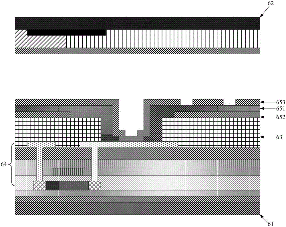
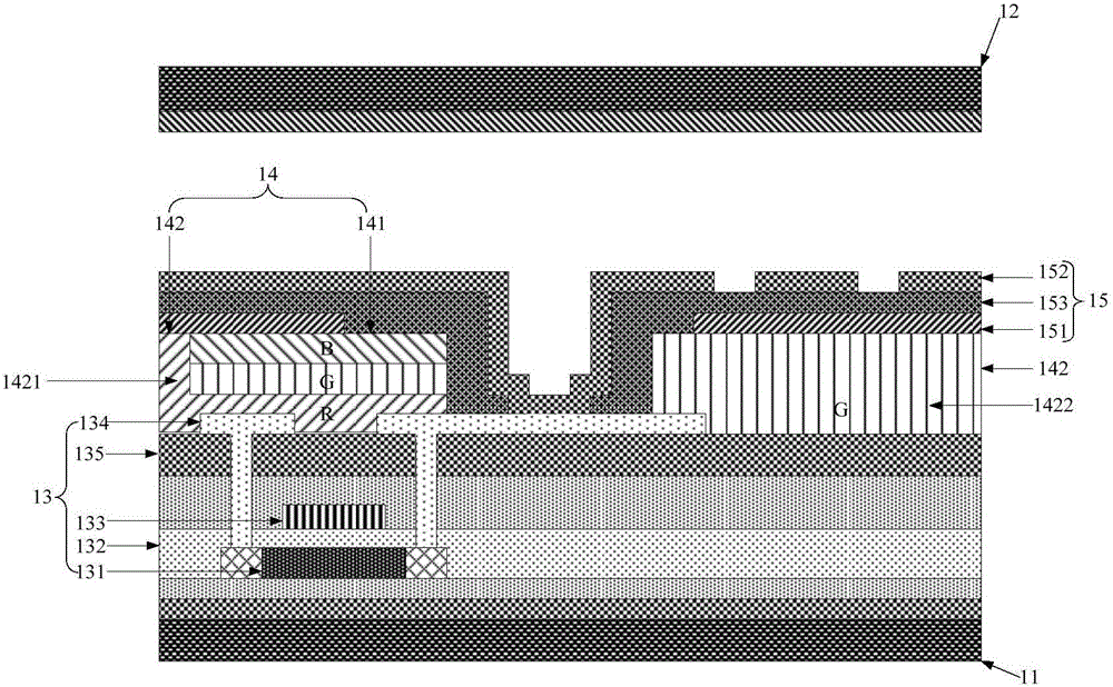
[0033] see figure 2 , figure 2 It is a structural schematic diagram of the first embodiment of the liquid crystal panel of the present invention.

[0034] The liquid crystal panel of the present invention includes a first substrate 11 , a second substrate 12 and a liquid crystal layer (not shown) between the first substrate 11 and the second substrate 12 .

[0035] A TFT array layer 13 , a color resist layer 14 and an electrode structure layer 15 are sequentially provided on the first substrate 11 .

[0036] The color resist layer 14 is formed by various color resists, the color resist layer includes a light-shielding area 141 and a plurality of pixel areas 142, the light-shielding area 141 is in a matrix shape, the plurality of pixel areas 142 are separated by the light-shielding area 141, and each pixel area 142 includes a different ki...


PUM


Abstract

The invention provides a liquid crystal display panel, a manufacturing method thereof and a display. The liquid crystal display panel comprises a first substrate, a second substrate and a liquid crystal layer positioned between the first substrate and the second substrate, wherein a TFT array layer, a color resistance layer and an electrode structure layer are sequentially arranged on the first substrate; the color resistance layer is formed by multiple color resistors and comprises a shading region and a plurality of pixel regions; the shading region is matrix-shaped; the plurality of pixel regions are separated by the shading region; each pixel region comprises a color resistor; and the shading region is formed by stacking multiple color resistors. According to the invention, the process can be simplified, the material cost and manufacturing time are saved, the aligning and pressing accuracy can be improved, and the product quality is further improved.

Description

technical field [0001] The invention relates to the technical field of liquid crystal display, in particular to a liquid crystal panel, a manufacturing method thereof and a display. Background technique [0002] With the wide application of liquid crystal displays, high resolution has become a development trend. In order to increase the aperture ratio of high resolution pixels, a low temperature polysilicon (LTPS, Low Temperature Poly-silicon) process has been developed and used. [0003] Such as figure 1 as shown, figure 1 It is a structural schematic diagram of an existing LTPS liquid crystal display panel. The existing LTPS liquid crystal display panel includes: an array substrate 61 (array substrate) and a color filter substrate 62 (CF substrate). The wires are planarized after fabrication, and the flat layer 63 is PL, wherein the PL can be a transparent material, such as a transparent resin. An insulating layer 651 , a common electrode 652 (common electrode), a pixe...

Claims


Application Information

Patent Timeline
Patent Type & Authority Applications(China)
IPC IPC(8): G02F1/1362
CPCG02F1/136209G02F1/136286G02F1/136295G02F1/13394G02F1/13396G02F1/136222G02F1/133345G02F1/1368G02F2201/121G02F2201/123
Inventor 唐岳军
Owner WUHAN CHINA STAR OPTOELECTRONICS TECH CO LTD
Why Eureka
Try Eureka