Array substrate and manufacturing method thereof and display device

a manufacturing method and array substrate technology, applied in the field of array substrates and manufacturing methods thereof, can solve the problems of large number of processes, complex manufacturing process, and defect in the manufacture of array substrates, and achieve the effect of reducing leakage curren

Inactive Publication Date: 2015-10-29
ORDOS YUANSHENG OPTOELECTRONICS +1
View PDF15 Cites 38 Cited by
  • Summary
  • Abstract
  • Description
  • Claims
  • Application Information

AI Technical Summary

Benefits of technology

[0050]For example, at least one light blocking metal layer is formed in the step of forming a pattern containing the data line and the common electrode line, at least one gate electrode is formed in the step of forming the ga

Problems solved by technology

From the above description with respect to the method for manufacturing the array substrate based on thin film transistors made of low temperature poly-silicon in the prior art, it can be seen that although the common electrode line 201 and the gate electrode 106 are formed by using a single exposure process,

Method used


Image

  • Array substrate and manufacturing method thereof and display device
  • Array substrate and manufacturing method thereof and display device
  • Array substrate and manufacturing method thereof and display device

Examples


third embodiment

[0098]the invention provides a manufacturing method of an array substrate, which comprises a step of forming data lines, scan lines, common electrodes and common electrode lines and a step of forming thin film transistors, the step of forming a thin film transistor comprises a step of forming a gate electrode, a source electrode, a drain electrode and an active layer, each of pixel regions defined by the scan lines and the data lines has a common electrode, a common electrode line and a thin film transistor, wherein, the data line and the common electrode line are formed in the same layer on the base substrate and below the active layer, a connection part is provided in the same layer as the common electrode and at least partly overlaps with the common electrode line in an orthographic projection direction, the common electrode is electrically connected to the common electrode line through a first via formed between the connection part and the common electrode line.

[0099]In the actu...

first embodiment

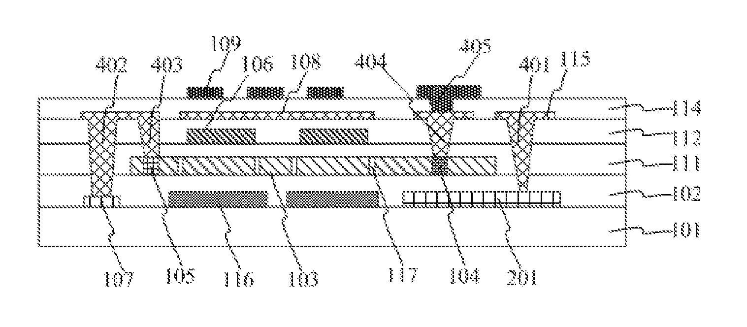
[0129]Through above steps, the array substrate provided in the invention, the structure of which is as shown in FIG. 12, may be manufactured.

second embodiment

[0130]A manufacturing method of the array substrate in the invention comprises:

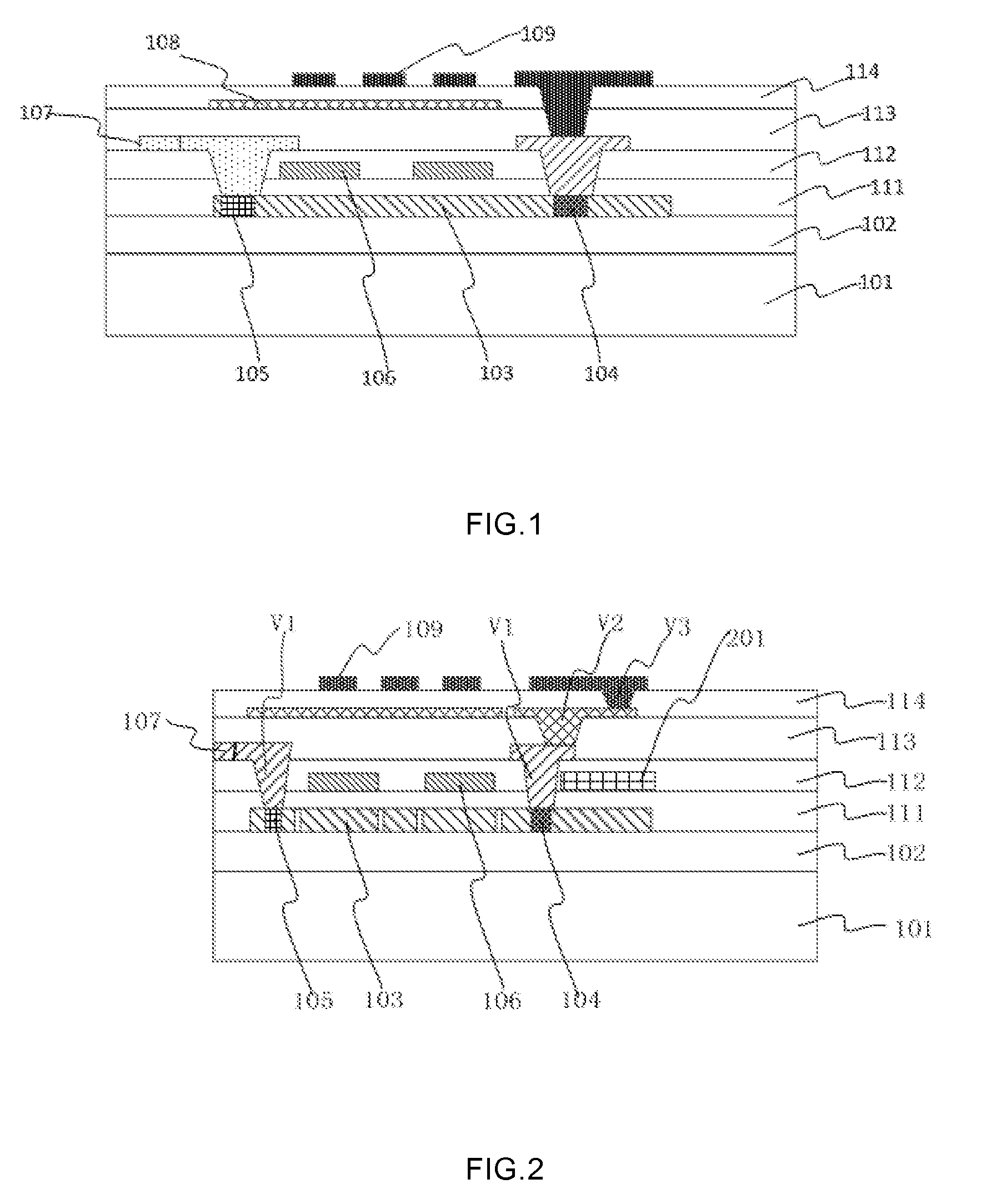
[0131]a first step, as shown in FIG. 14, depositing a layer of metal thin film on the base substrate 101, then forming a pattern containing data lines 107, a light blocking metal layer 116 and a common electrode line 201 through a first patterning process, wherein the data lines 107, the light blocking metal layer 116 and the common electrode line 201 are provided separately.

[0132]a second step, with reference to FIG. 15, forming a buffer layer 102 on the base substrate subjected to the first step, wherein the buffer layer 102 completely covers the data lines 107, the light blocking metal layer 116 and the common electrode line 201.

[0133]a third step, with reference to FIG. 15, on the base substrate 101 subjected to the second step, forming a pattern including a low temperature poly-silicon active layer 103 by using a second patterning process. The active layer 103 is formed on the buffer layer 102, and t...


PUM


Abstract

The invention discloses an array substrate and a manufacturing method thereof and a display device, which can solve the problems such as complicated, high cost, time-consuming process in the prior art, and increase the storage capacitance. In the array substrate, data lines and a common electrode line are provided in the same layer on the base substrate and below an active layer, the data lines and the common electrode line are provided separately, the common electrode is provided with a connection part which partly overlaps with the common electrode line in an orthographic projection direction, and the common electrode is electrically connected to the common electrode line through a first via between the connection part and the common electrode line.

Description

FIELD OF THE INVENTION[0001]The invention relates to the field of display technology, and in particular, to an array substrate and a manufacturing method thereof and a display device.BACKGROUND OF THE INVENTION[0002]The amorphous silicon is limited in many fields because of its low on-state current, low Mobility, and poor stability due to its own defects, in order to compensate for the defects of the amorphous silicon of its own so as to be used widely in related fields, a low temperature poly-silicon(LTPS) is proposed.[0003]With the development of the thin film transistor liquid crystal display (TFT-LCD) technology, a display technology based on the low temperature poly-silicon has become a mainstream. As shown in FIG. 1, in the prior art, an array substrate based on thin film transistors made of low temperature poly-silicon comprises: a base substrate 101, a buffer layer 102, an active region 103, a gate electrode 106, a source electrode 105, a drain electrode 104, a data line 107...

Claims


Application Information

Patent Timeline
IPC IPC(8): H01L27/12H01L29/786H01L21/28H01L29/66
CPCH01L27/1222H01L29/6675H01L21/28H01L27/127H01L29/78621H01L27/124G02F1/136227G02F1/136286G02F1/1333G02F1/1368
Inventor SUN, JIANLI, CHENGAN, SEONGJUNRYU, BONGYEOL
Owner ORDOS YUANSHENG OPTOELECTRONICS
Why Eureka
Try Eureka