
Semiconductor device

A semiconductor and flip-chip technology, which is applied in semiconductor devices, semiconductor/solid-state device parts, electric solid-state devices, etc., can solve problems such as stripping of heat sinks

Active Publication Date: 2016-08-17
AMKOR TECH JAPAN INC
View PDF10 Cites 6 Cited by
  • Summary
  • Abstract
  • Description
  • Claims
  • Application Information

AI Technical Summary

Problems solved by technology

[0007] However, there may be a problem that the heat dissipation plate provided for improving heat dissipation may be peeled off due to the stress accompanying thermal expansion or thermal contraction.

Method used


Image

  • Semiconductor device
  • Semiconductor device
  • Semiconductor device

Examples


Embodiment approach 1

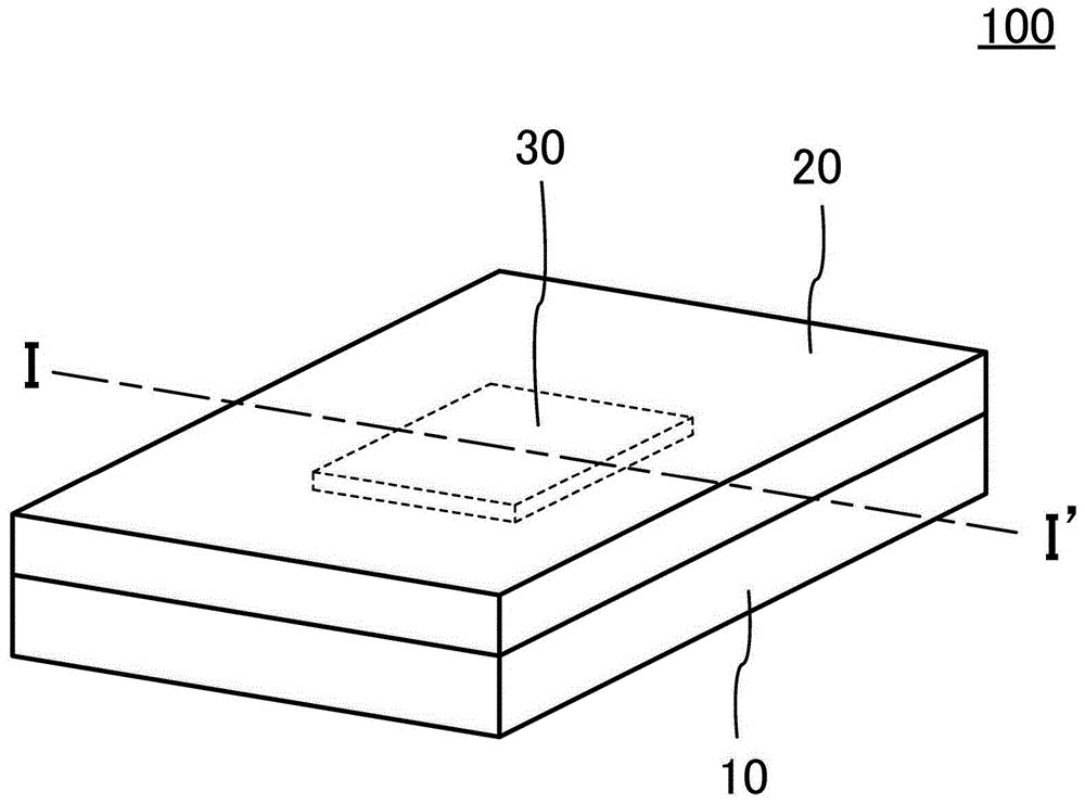
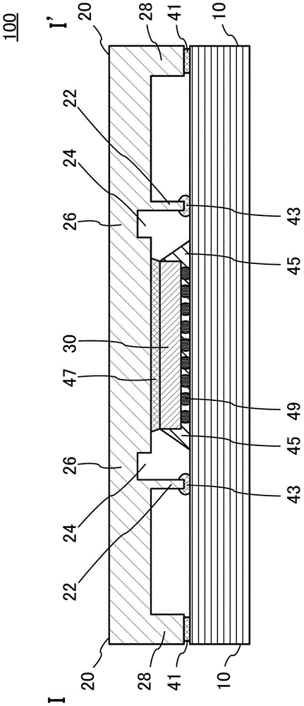
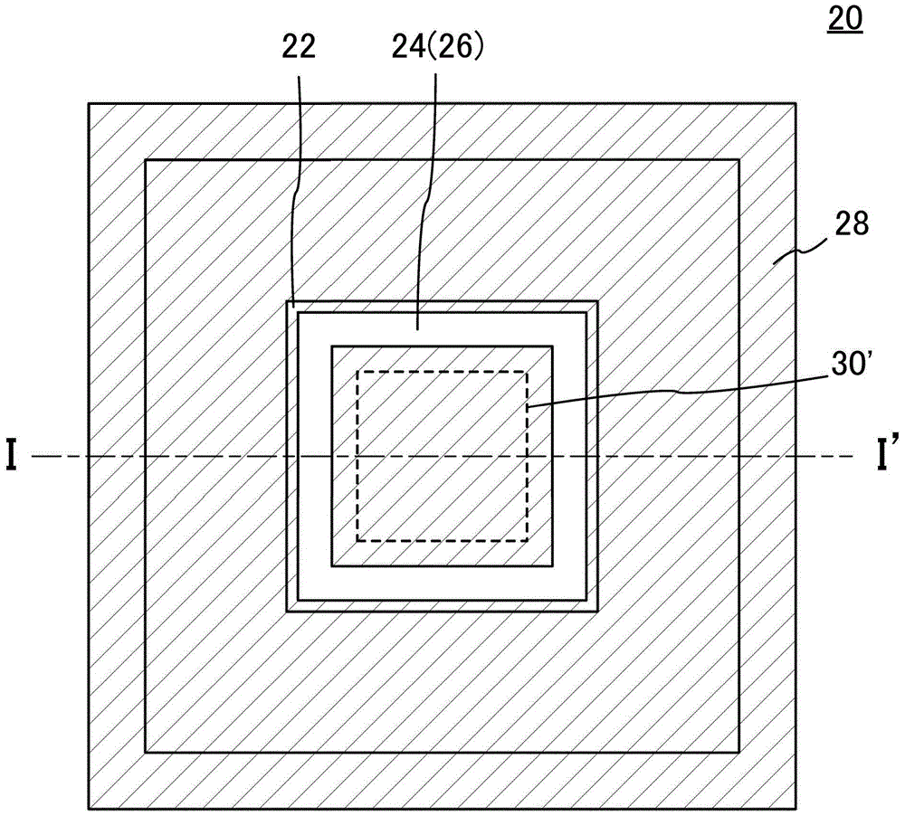
[0035] use figure 1 Referring to FIG. 3 , the structure of the semiconductor device according to Embodiment 1 will be described.

[0036] [Overall structure of semiconductor device]

[0037] figure 1 It is a schematic diagram showing the overall structure of the semiconductor device 100 according to the first embodiment of the present invention. In the semiconductor device 100 , a semiconductor chip 30 is arranged on a substrate 10 , and a heat sink 20 is arranged on the substrate 10 and the semiconductor chip 30 . The substrate 10 and the radiator plate 20 are disposed opposite to each other, and both have substantially the same area, and the semiconductor device 100 has a substantially cubic shape.

[0038] [Cross-sectional view of a semiconductor device]

[0039] figure 2 To show the edge of the semiconductor device 100 according to the first embodiment of the present invention figure 1 The cross-sectional view of the line I-I'.

[0040] The substrate 10 is a packag...

no. 2 approach

[0052] For an overview of the semiconductor device according to the second embodiment of the present invention, refer to Figure 4A and Figure 4B to explain.

[0053] Figure 4A It is a plan view of the heat sink 20 of the semiconductor device of the second embodiment, Figure 4B for along Figure 4A The cross-sectional view of the II-I' line in . The second embodiment is characterized in that two grooves, ie, groove 24 a and groove 24 b are arranged in heat dissipation plate 20 , and stress absorbing portion 26 is formed. The groove 24a and the groove 24b are formed between the region 30' where the semiconductor chip 30 is bonded and the protrusion 22. As with the groove 24 of the first embodiment, it is preferable that the groove 24 a be arranged close to the position where the protrusion 22 is arranged. More preferably, the groove 24a is arranged adjacent to the position where the protrusion 22 is arranged. In addition, like the groove 24 of the first embodiment, th...

no. 3 approach

[0056] For an overview of the semiconductor device according to the third embodiment of the present invention, refer to Figure 5A and Figure 5B to explain.

[0057] Figure 5A It is a plan view of the heat sink 20 of the semiconductor device of the third embodiment, Figure 5B for along Figure 5A The cross-sectional view of the II-I' line in . The third embodiment is characterized in that a bottom hole 24 c is arranged in the radiator plate 20 to form a stress absorbing portion 26 . The bottomed hole 24c is formed between the region 30' where the semiconductor chip 30 is bonded and the protrusion 22. Preferably, the bottomed hole 24c is disposed near the position where the protruding portion 22 is disposed. More preferably, the bottomed hole 24c is arranged adjacent to the position where the protrusion 22 is arranged. refer to Figure 5A It can be seen that the plurality of bottomed holes 24c are arranged at predetermined intervals along the protrusion 22 and arrang...


PUM


Abstract

The objective of the invention is to overcome a problem that an adhesion part between a heat sink and a substrate peels off because the heat sink configured to a semiconductor chip and the substrate expands or contracts along with heat. A semiconductor device includes a substrate whose surface is made of an insulation material, a semiconductor chip flip-chip connected on the substrate, and a heat sink bonded to the semiconductor chip via a thermal interface material and fixed to the substrate outside the semiconductor chip, wherein the heat sink has a protrusion part protruding toward the substrate and bonded to the substrate via a conductive resin between a part bonded to semiconductor chip and a part fixed to the substrate and the heat sink has a stress absorbing part. According to the semiconductor device, the protrusion part of the heat sink is prevented from being peeled off due to heat expansion or heat contraction from the substrate at the part where the protrusion part of the heat sink is bonded to the substrate.

Description

technical field [0001] The present invention relates to semiconductor devices, and more particularly to the art of flip-chip bonded (FCB) packages with low-stress heat sinks. Background technique [0002] As the speed of semiconductor devices increases and the number of input / output (I / O) increases, the amount of heat generated from semiconductor devices also increases. Accordingly, there is known a semiconductor package in which a heat sink is bonded to a semiconductor chip. In addition, it is known to stabilize the ground by connecting the heat sink to the ground of the package substrate for the purpose of reducing the noise of high-speed devices. [0003] For example, a semiconductor device is disclosed in which a heat dissipation member is embedded in a sealing member that embeds a semiconductor chip in order to improve heat dissipation (for example, refer to Patent Document 1). According to the semiconductor device disclosed in Patent Document 1, if the surface area o...

Claims


Application Information

Patent Timeline
Patent Type & Authority Applications(China)
IPC IPC(8): H01L23/367
CPCH01L23/3672H01L23/373H01L23/04H01L23/10H01L24/13H01L24/16H01L24/29H01L2224/13101H01L2224/13139H01L2224/13144H01L2224/13147H01L2224/2919H01L2224/29193H01L2224/32225H01L2224/73204H01L2924/10253H01L2924/10272H01L2924/1033H01L2924/14H01L2924/16153H01L2924/1616H01L23/3675H01L23/3736H01L24/32H01L24/73H01L23/562H01L2224/73253H01L2224/32245H01L2924/014H01L2924/00014H01L2924/0655H01L2924/07025H01L2924/0715H01L2924/0635H01L2924/0675H01L2224/16225H01L2924/00H01L21/563H01L24/17H01L2924/01029H01L2924/01013H01L2924/01014H01L2924/059H01L2924/3511
Inventor 广部正雄
Owner AMKOR TECH JAPAN INC
Learn More