Method for enhancing adhesion of photoresist after developing

A photoresist and adhesion technology, applied in photosensitive material processing, electrical components, semiconductor/solid-state device manufacturing, etc., can solve problems such as photoresist peeling, improve process latitude, and solve the problem of photoresist peeling. Effect

Inactive Publication Date: 2018-04-20
SHANGHAI HUAHONG GRACE SEMICON MFG CORP
View PDF7 Cites 4 Cited by
  • Summary
  • Abstract
  • Description
  • Claims
  • Application Information

AI Technical Summary

Problems solved by technology

[0004] The technical problem to be solved by the present invention is to provide a method for enhancing the adhesiveness of the photoresist after development, so as to solve the problem of peeling off the photoresist during high-dose injection

Method used


Image

  • Method for enhancing adhesion of photoresist after developing

Examples


Embodiment Construction

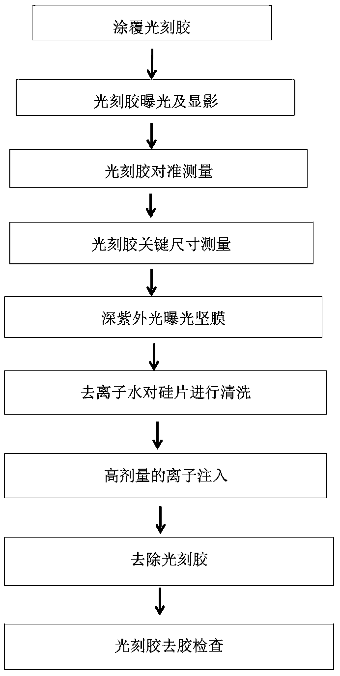
[0020] The method for enhancing photoresist adhesion after development of the present invention comprises the following process steps:

[0021] The first step is to coat the photoresist; the positive or negative photoresist is evenly coated on the surface of the silicon wafer by spin coating, and the hard film is baked.

[0022] In the second step, the photoresist is exposed and developed to complete the pattern transfer.

[0023] The third step is photoresist alignment measurement.

[0024] The fourth step is photoresist critical dimension (CD) measurement.

[0025] The fifth step is to expose the hardened film to UVQ with deep ultraviolet light.

[0026] In the sixth step, the silicon wafer is cleaned and infiltrated with deionized water.

[0027] The seventh step is to perform high-dose ion implantation.

[0028] In the eighth step, the photoresist is removed by a plasma stripping method.

[0029] The ninth step is to check the photoresist removal.

[0030] Through th...


PUM


Abstract

The invention discloses a method for enhancing adhesion of a photoresist after developing. The method comprises the steps of 1, performing coating on the photoresist; 2, performing exposure and developing on the photoresist; 3, performing aligned measurement on the photoresist; 4, performing critical dimension measurement on the photoresist; 5, performing UVQ; 6, performing cleaning and wetting ona silicon wafer by deionized water; 7, performing high-dosage ion injection; 8, removing the photoresist; and 9, performing adhesive-removing examination on the photoresist. According to the method for enhancing adhesion of the photoresist after developing, cleaning and wetting of the silicon wafer by deionized water is added after the photoresist is completely developed, so that high adhesion between the photoresist and the silicon wafer can be ensured, the problem of photoresist peeling in high-dosage injection can be solved, and process margin is improved.

Description

technical field [0001] The invention relates to the field of semiconductor manufacturing, in particular to a method for enhancing the adhesion of photoresist after development. Background technique [0002] The photolithography process is an important step in the semiconductor manufacturing process and is the primary method for transferring design layouts onto silicon wafers. The essence of photolithography is to copy the temporary circuit structure to the silicon wafer that will be etched and ion-implanted later. These structures are first made in the form of graphics only on the quartz template called the mask. Ultraviolet light passes through the mask to transfer the pattern to the photosensitive film on the surface of the silicon wafer. The usual photolithography is carried out in this way: firstly, the photoresist is spin-coated on the cleaned and dehydrated silicon wafer, and after the film is softly baked, it is aligned and exposed, then baked and developed, and the ...

Claims


Application Information

Patent Timeline
Patent Type & Authority Applications(China)
IPC IPC(8): G03F7/26G03F7/40H01L21/02
CPCG03F7/26G03F7/40H01L21/02057
Inventor 宗立超王星杰
Owner SHANGHAI HUAHONG GRACE SEMICON MFG CORP
Why Eureka
Try Eureka