

Reference voltage generation circuit with temperature compensating function
A voltage generation circuit and reference voltage technology, applied in the direction of adjusting electrical variables, control/regulating systems, instruments, etc., can solve the problems of circuit performance impact, poor matching, and monotonicity of the later stage, and reduce system power consumption, Optimizing the effect of matching
Patent Information
- Authority / Receiving Office
- CN · China
- Patent Type
- Applications(China)
- Current Assignee / Owner
- Publication Date
- 2016-08-24
Smart Images
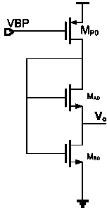
Figure 1 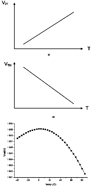
Figure 2 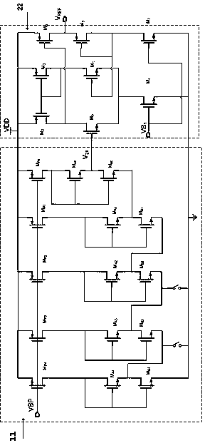
Figure 3
Abstract
Description
technical field
[0001] The invention relates to the technical field of reference voltage sources, in particular to a reference voltage generation circuit with temperature compensation function. Background technique
[0002] The voltage reference source is one of the indispensable components in many circuit systems. It is often used to provide a low temperature coefficient reference voltage for high-performance analog circuits or digital circuit modules to improve the performance of the circuit.
[0003] In the prior art, in the field of integrated circuits, traditional voltage reference source circuits usually use a bandgap reference circuit composed of classic bipolar transistors. The basic principle is that the base-emitter junction of bipolar crystals has negative temperature characteristics ; On the other hand, when the collector currents of bipolar transistors are different, the temperature curves of the base-emitter junctions are different. When different currents flow...
Examples
Embodiment Construction
[0015] The reference voltage generation circuit with temperature compensation function of the present invention includes a positive temperature coefficient voltage generation circuit 11 and an LDO-like circuit 22 connected in sequence. After the voltage with positive temperature coefficient output by the positive temperature coefficient voltage generating circuit 11 is superimposed on the voltage with negative temperature coefficient by the LDO-like circuit 22 , the output end of the LDO-like circuit 22 outputs a reference voltage Vref with a low temperature coefficient. The positive temperature coefficient voltage generating circuit 11 is composed of single-level or multi-level unit circuits, and each unit circuit includes a bias current source P using MOS transistors and two NMOS transistors. The unit circuits at all levels are sequentially cascaded, and the gate of NMOS transistor A in each level of unit circuit is connected to the gate of NMOS transistor B, and then respect...