Power module structure and manufacture method thereof

A technology for power modules and manufacturing methods, which is applied in semiconductor/solid-state device manufacturing, semiconductor/solid-state device components, semiconductor devices, etc., can solve problems such as joint damage, low power density of power modules, chip failure, etc., and saves layout. area, increase power density, and realize the effect of compactness and miniaturization

Inactive Publication Date: 2016-08-31
ZHUZHOU CSR TIMES ELECTRIC CO LTD
View PDF5 Cites 5 Cited by
  • Summary
  • Abstract
  • Description
  • Claims
  • Application Information

AI Technical Summary

Problems solved by technology

The two-dimensional planar chip layout is not conducive to the compactness and miniaturization of the power module, which is not conducive to improving the power density of the power module, and usually produces large thermal stress, resulting in deflection, fracture or joint damage, which is easy to cause the chip to fail
[0004] In existing power modules, the main switching device (such as IGBT or MOSFET) and the freewheeling diode (such as FRD or SiC SBD) are arranged side by side on the same plane, which makes the power density of the power module relatively small

Method used


Image

  • Power module structure and manufacture method thereof
  • Power module structure and manufacture method thereof
  • Power module structure and manufacture method thereof

Examples


Embodiment Construction

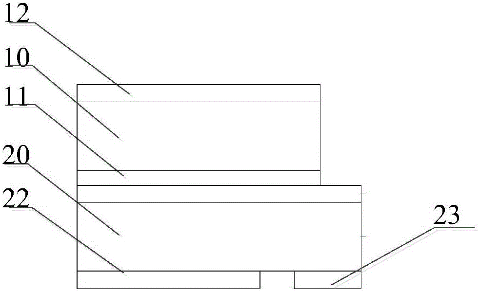
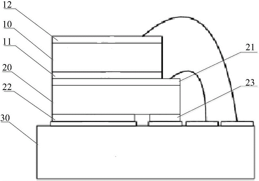
[0029] As mentioned in the background technology section, in the prior art, the main switching device (such as IGBT or MOSFET) and the freewheeling diode (such as FRD or SiC SBD) are arranged side by side on the same plane in the existing power module, so that the power module The power density is too small.

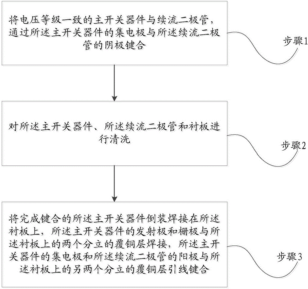
[0030] Based on this, an embodiment of the present invention provides a power module structure, including a main switching device, a freewheeling diode and a substrate, the voltage level of the main switching device and the freewheeling diode are consistent, and the current magnitude is the same. After the collector of the switching device is bonded to the cathode of the freewheeling diode, the main switching device is flip-chip welded on the backing board, and the backing board is provided with a plurality of discrete copper clad layers, wherein the The emitter of the main switching device is welded to the first copper clad layer on the lining board, the gate is welded ...


PUM


Abstract

The present invention discloses a power module structure and a manufacture method thereof. The power module structure comprises: a main switch device has the same voltage grade with a freewheeling diode, and has the same size of the current with the freewheeling diode; the collector of the main switch device is bonded with the cathode of the freewheeling diode, and the main switch device is welded on a liner plate in an inverted mode; the liner plate is provided with a plurality of discrete copper-cladding layer; the emitting electrode of the main switch device is welded with the first copper-cladding layer of the liner plate, and a grid is welded with the second copper-cladding layer on the liner plate; and the collector outgoing line of the main switch device is bonded with the third copper-cladding layer of the liner plate, and the anode outgoing line of the freewheeling diode is bonded with the fourth copper-cladding layer on the liner plate. The power module structure and manufacture method thereof realize the compaction and the miniaturization and improve the power density of the power module through welding the bonded main switch device and the freewheeling diode on the liner plate.

Description

technical field [0001] The invention relates to the technical field of semiconductors, in particular to a power module structure and a manufacturing method. Background technique [0002] In recent years, as power electronic devices such as insulated gate bipolar transistors (IGBTs) and silicon carbide (SiC) devices have become more and more widely used, such as inverters on electric vehicles, drives on trains, engines, and wind power generator etc. In order to achieve compactness, miniaturization, high frequency, high power density and high integration of power electronic devices, packaging technology needs to be greatly improved. Traditionally, power semiconductor devices mostly adopt a two-dimensional planar chip layout, and main switching devices such as IGBTs and freewheeling diodes are arranged side by side on the same plane. The two-dimensional planar chip layout is not conducive to the compactness and miniaturization of the power module, which is not conducive to im...

Claims


Application Information

Patent Timeline
Patent Type & Authority Applications(China)
IPC IPC(8): H01L25/18H01L23/495H01L25/00H01L21/60
CPCH01L24/83H01L25/18H01L25/50H01L23/4951H01L2224/83379H01L2224/83365H01L2224/32145H01L2224/48091H01L2224/73265H01L2924/00014
Inventor 李诚瞻常桂钦彭勇殿冯江华刘国友
Owner ZHUZHOU CSR TIMES ELECTRIC CO LTD
Why Eureka
Try Eureka