Single-barrier type InGaAsSb infrared detector

A technology of infrared detectors and potential barriers, applied in semiconductor devices, electrical components, circuits, etc., can solve the problem of small dark current

Inactive Publication Date: 2016-09-07
INST OF SEMICONDUCTORS - CHINESE ACAD OF SCI
View PDF3 Cites 4 Cited by
  • Summary
  • Abstract
  • Description
  • Claims
  • Application Information

AI Technical Summary

Problems solved by technology

[0005] The purpose of the present invention is to provide a single barrier type InGaAsSb infrared detector to address the defects of current

Method used


Image

  • Single-barrier type InGaAsSb infrared detector
  • Single-barrier type InGaAsSb infrared detector
  • Single-barrier type InGaAsSb infrared detector

Examples


Embodiment 1

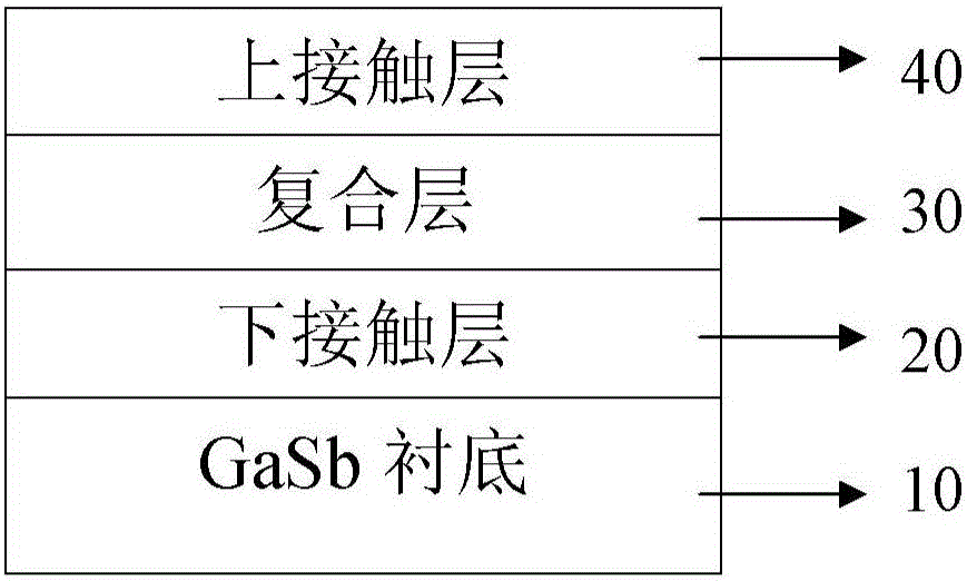
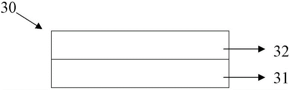
[0025] to combine figure 1 and figure 2 Describe this embodiment, combine figure 1 To illustrate this embodiment, an InGaAsSb barrier detector with a cut-off wavelength of 2.7 μm is sequentially grown on an N-type GaSb substrate 10 with a thickness of 1.5 μm and a P-type doping concentration of 2×10 by using an MBE system. 18 cm -3 The GaSb used as the lower contact layer 20 is used to prepare the lower electrode contact, and the wiring leads to form the lower electrode of the detector; unintentional doping, Al with a thickness of 0.4 μm 0.5 Ga 0.5 As 0.05 Sb 0.95 Barrier layer 32, its role is to hinder dark current, reduce noise, and because of its energy band structure characteristics, it will not hinder photogenerated carriers; unintentional doping, In with a thickness of 2 μm 0.27 Ga 0.83 As 0.25 Sb 0.85 The light absorbing layer 31 is used to absorb photogenerated carriers; the N-type doping concentration is 2×10 18 cm -3 , a thickness of 0.5 μm of In 0.27 Ga...

Embodiment 2

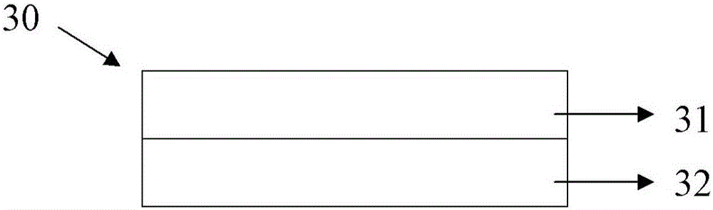
[0027] An InGaAsSb barrier detector with a cutoff wavelength of 2.7 μm, using an MBE system to sequentially grow N-type doping concentration of 2×10 with a thickness of 0.5 μm on an N-type GaSb substrate 10 18 cm -3 In 0.27 Ga 0.83 As 0.25 Sb 0.85 As the lower contact layer 20, in order to be used for preparing the lower electrode contact, the wiring leads out to form the lower electrode of the detector; unintentionally doped, with a thickness of 2 μm In 0.27 Ga 0.83 As 0.25 Sb 0.85 Light absorbing layer 31 for absorbing light; unintentionally doped, Al with a thickness of 0.4 μm 0.5 Ga 0.5 As 0.05 Sb 0.95 The barrier layer 32 is used to hinder dark current and reduce noise, and at the same time, due to its energy band structure, it will not hinder photogenerated carriers; the N-type doping concentration is 2×10 18 cm -3 , a thickness of 0.5 μm of In 0.27 Ga 0.83 As 0.25 Sb 0.85 The upper contact layer 40 is used to prepare the upper electrode contact, and the ...


PUM

PropertyMeasurementUnit
Thicknessaaaaaaaaaa

Abstract

Disclosed is a single-barrier type InGaAsSb infrared detector. The detector comprises a GaSb substrate, a lower contact layer which is manufactured on the GaSb substrate, a composite layer which is manufactured on the lower contact layer, and an upper contact layer which is manufactured on the composite layer. For overcoming the shortcomings of the existing strain InGaAs detector, the invention provides the single-barrier type InGaAsSb infrared detector with the advantages of low dark current and low noise.

Description

technical field [0001] The invention relates to the technical field of photodetectors, in particular to a single barrier type InGaAsSb infrared detector which can output 2-3 μm infrared photodetectors. Background technique [0002] 2-3μm infrared photodetectors have a wide range of uses. Infrared rays in this wavelength range can penetrate smoke well, and atmospheric glow imaging can also be used at night, which has important applications in military and remote sensing. [0003] At present, most 2-3μm infrared detectors use extended-wavelength strained InGaAs epitaxially grown on InP substrates. InGaAs with a high In composition does not match the InP substrate lattice, and a large amount of InGaAs is generated during the relaxation process during growth. Therefore, a large amount of dark current is generated when the device is working, which makes it difficult to improve the performance of the device. [0004] On the GaSb substrate, epitaxy of InGaAsSb that matches its lat...

Claims


Application Information

Patent Timeline
IPC IPC(8): H01L31/109H01L31/0304
CPCH01L31/109H01L31/03046
Inventor 向伟王国伟徐应强郝宏玥韩玺任正伟贺振宏牛智川
Owner INST OF SEMICONDUCTORS - CHINESE ACAD OF SCI
Why Eureka
Try Eureka