Sandwich structure for ultrathin laminated board processing and laminated board manufacturing method

A multi-layer board and sandwich technology, which is applied in the direction of multi-layer circuit manufacturing, printed circuit manufacturing, and simultaneous processing of multiple printed circuits. Difficulty and other problems, to achieve the effect of good symmetry, reducing process difficulty and simplifying process

Active Publication Date: 2016-09-07
NAT CENT FOR ADVANCED PACKAGING
View PDF5 Cites 10 Cited by
  • Summary
  • Abstract
  • Description
  • Claims
  • Application Information

AI Technical Summary

Problems solved by technology

Although this method can achieve through-hole plating, the process is difficult and there are two problems:
[0008] 2. The alignment accuracy of the small holes on the front and back sides is high. If the front and back sides are misaligned, it will affect the electroplating
It can be seen that the control of this kind of processing technology is difficult, and the consistency and repeatability and environmental requirements are high.

Method used


Image

  • Sandwich structure for ultrathin laminated board processing and laminated board manufacturing method
  • Sandwich structure for ultrathin laminated board processing and laminated board manufacturing method
  • Sandwich structure for ultrathin laminated board processing and laminated board manufacturing method

Examples


Embodiment Construction

[0055] The present invention will be further described below in conjunction with specific drawings and embodiments.

[0056] This embodiment introduces the sandwich structure for processing ultra-thin multilayer boards, and the method for making multilayer boards by using the sandwich structure for processing ultra-thin multilayer boards;

[0057] A method for making a multilayer board, comprising the steps of:

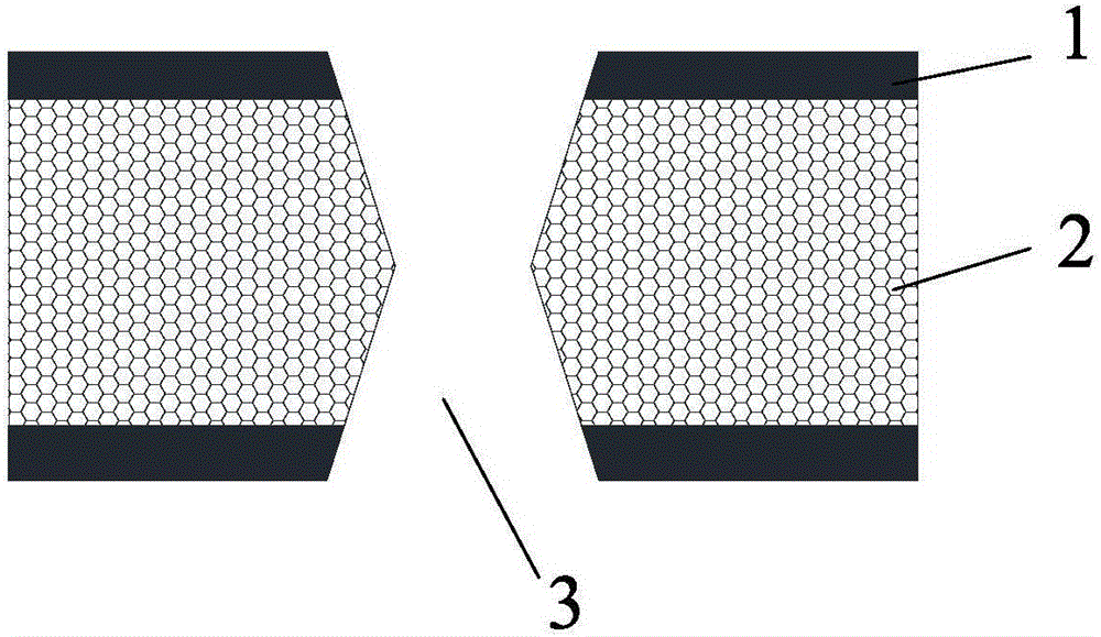
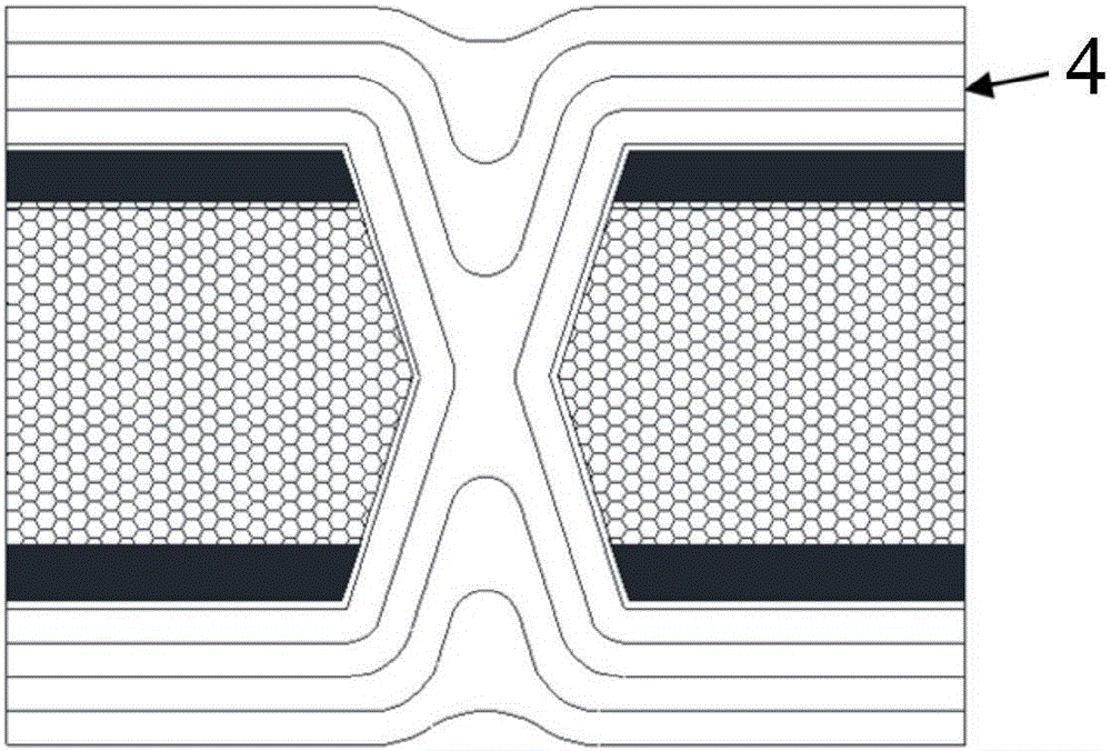
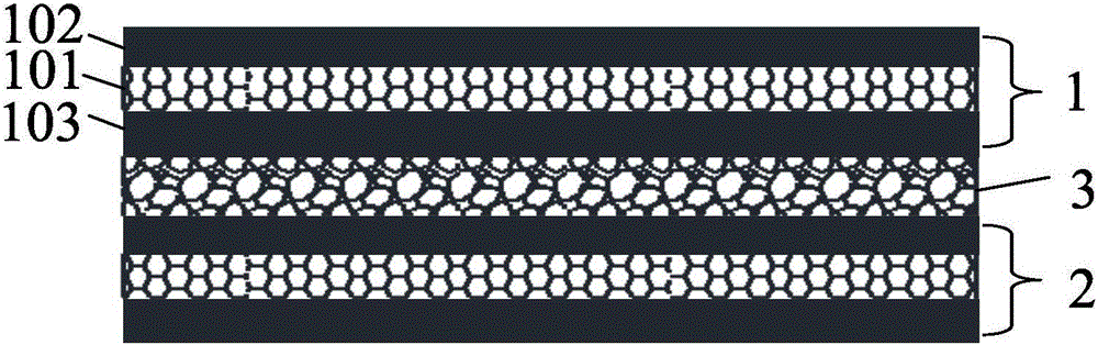
[0058] Step S1, providing two ultra-thin double-sided copper-clad laminates 1 and 2; placing the first prepreg 3 between the two double-sided copper-clad laminates 1 and 2, and pressing at low temperature to form a three-layer temporary bonding structure, wherein the first prepreg 3 is not Curing; the temperature of low temperature lamination is 80℃~140℃; image 3 shown;

[0059] Ultra-thin double-sided copper-clad laminates in this example refer to double-sided copper-clad laminates below 80 μm;

[0060] The prepreg used in the present invention can be the prepreg o...


PUM


Abstract

The invention provides a method for manufacturing laminated board. The method comprises the following steps: firstly laminating two double-sided copper-clad boards on an upper surface and a lower surface of one bearing plate board at low temperature at a second prepreg and a third prepreg so as to form a sandwich structure for the ultrathin laminated board processing; forming blind holes on the two double-sided copper-clad boards on the upper surface and the lower surface of the sandwich structure for the ultrathin laminated board processing through laser drilling; forming the other surface circuit of each of two double-sided copper-clad boards on the structure of step S5 through metallization; laminating two outer layer copper foils on the upper surface and the lower surface of the sandwich structure for the ultrathin laminated board processing through a fourth prepreg and a fifth prepreg so as to form cured sandwich structure; forming two four-layer circuit board structures on the outside of a release film of the bearing board; and finally peeling off two four-layer circuit board structures on the outside of the release film of the bearing board. Through the adoption of the structure provided by the invention, the process difficulty can be reduced, two circuit boards are prepared at once, the efficiency is improved, and the warping problem produced in the base plate manufacturing is solved.

Description

technical field [0001] The invention relates to a processing technology, in particular to a processing technology of an ultra-thin circuit board with a thickness below 80 μm. Background technique [0002] The through-hole filling of circuit boards with a thickness of less than 80 μm is difficult to manufacture, and it is difficult to fill the holes by electroplating. Therefore, it is impossible to complete the stacked holes of multi-layer boards, and it is difficult to complete the problem of electroplating and filling holes. [0003] The processing of ultra-thin plates with a thickness below 80 μm will cause folded plates and jammed plates when processed on the usual horizontal line of the substrate, and in severe cases, it is easy to produce waste plates. [0004] At present, double-sided copper-clad laminates with a thickness of less than 80 μm can form through-holes with a diameter of less than 100 μm on the copper-clad laminates by laser drilling, and this small through...

Claims


Application Information

Patent Timeline
Patent Type & Authority Applications(China)
IPC IPC(8): H05K3/46H05K3/00
CPCH05K3/0097H05K3/46H05K2203/107H05K2203/1484
Inventor 于中尧郭学平方志丹
Owner NAT CENT FOR ADVANCED PACKAGING
Why Eureka
Try Eureka