Semiconductor device

一种半导体、导通的技术,应用在半导体器件、半导体/固态器件制造、逻辑电路接口装置等方向,能够解决半导体装置破坏等问题

Active Publication Date: 2016-09-14
FUJI ELECTRIC CO LTD
View PDF7 Cites 4 Cited by
  • Summary
  • Abstract
  • Description
  • Claims
  • Application Information

AI Technical Summary

Problems solved by technology

Therefore, a large current flows from the ground potential terminal to the semiconductor device due to the negative voltage surge, and the semiconductor device may be destroyed by the large current.

Method used


Image

  • Semiconductor device
  • Semiconductor device
  • Semiconductor device

Examples


Embodiment Construction

[0059] Hereinafter, a semiconductor device according to one embodiment of the present invention will be described with reference to the drawings.

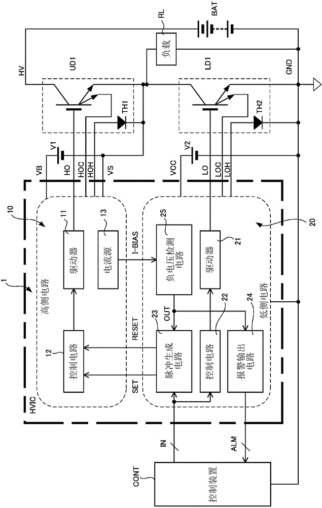
[0060] figure 1 It is a diagram showing a semiconductor device and its peripheral circuits according to one embodiment of the present invention. The semiconductor device of this embodiment is formed as a high-voltage integrated circuit HVIC that complementarily turns on and off the first semiconductor switching element UD1 and the second semiconductor switching element LD1 that are connected in series to form a half-bridge circuit. break drive control.

[0061] Here, the first semiconductor switching element UD1 and the second semiconductor switching element LD1 include, for example, an IGBT including an emitter for current detection. The first semiconductor switching element UD1 and the second semiconductor switching element LD1 receive the driving signals HO, LO output from the semiconductor device 1 of the present invention fo...


PUM


Abstract

Provided is a semiconductor device comprising: a first circuit (10, a high-side circuit) that operates with a first potential (VS) being used as a reference potential; and a second circuit (20, a low-side circuit) that operates with a second potential (GND) different from the first potential (VS) being used as a reference potential, wherein it can be detected with reliability that a negative voltage has been applied to the first circuit (10). The high-side circuit (10) comprises a current source (13). The current source (13) supplies a current (I-BIAS) to the low-side circuit (20), and varies the current (I-BIAS) according to whether the first potential (VS) is a negative voltage relative to the second potential (GND). The low-side circuit (20) comprises a negative voltage detection circuit (25). The negative voltage detection circuit (25) monitors the variation of the current (I-BIAS) supplied from the current source (13) and detects that a negative voltage has been applied to the high-side circuit (10).

Description

technical field [0001] The present invention relates to a high-side circuit and a low-side circuit that control complementary on-off (on-off) driving of, for example, a first semiconductor switching element and a second semiconductor switching element forming a half-bridge circuit, particularly A semiconductor device capable of reliably detecting a negative voltage applied to the high-side circuit when the first semiconductor switching element is turned off. Background technique [0002] As a power supply device for driving an industrial motor or a server, it is known to include a first semiconductor switching element and a second semiconductor switching element connected in series to form a half-bridge circuit, and to supply the motor, etc., from the midpoint of the half-bridge circuit. A power supply unit that supplies power to a load. The first semiconductor switching element and the second semiconductor switching element in such a power supply device are constituted by,...

Claims


Application Information

Patent Timeline
Patent Type & Authority Applications(China)
IPC IPC(8): H03K17/687H01L21/822H01L27/04H02M1/00H03K5/08
CPCH03K17/165H03K17/18H03K2217/0027H02M1/08H03K5/08H01L27/0255H01L27/0629H01L29/866H03K17/08128H03K19/017509
Inventor 赤羽正志
Owner FUJI ELECTRIC CO LTD
Why Eureka
Try Eureka