Ordered large-area single-layer microspheres/nanospheres assisted by template and preparation method thereof
A large-area, nanosphere technology, applied in separation methods, chemical instruments and methods, and processes for producing decorative surface effects, etc., can solve problems such as unstable spectral response, lattice defects, and poor batch repeatability, and achieve Improve chaotic direction, reduce lattice defects, and achieve high order effect
- Summary
- Abstract
- Description
- Claims
- Application Information
AI Technical Summary
Problems solved by technology
Method used
Image

Examples
Embodiment 1
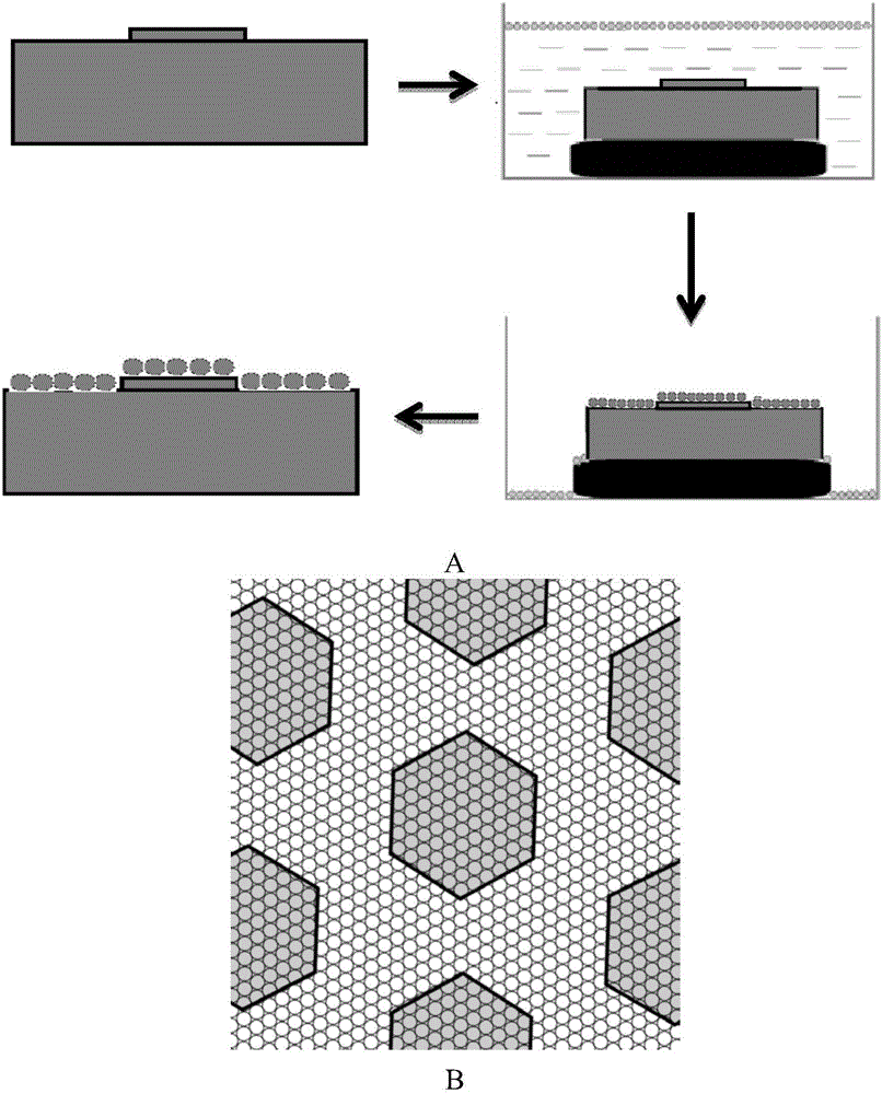
[0027] (1) Cut the 5-inch N-type silicon wafer into multiple small-sized silicon wafers of 3cm*3cm, and cut the glass slide into small pieces.
[0028] (2) Sonicate the cut silicon chip and slide glass in acetone, isopropanol, ethanol, and deionized water for 10 minutes respectively, and soak them in 5% hydrofluoric acid, then rinse them with deionized water, and Remove surface oil, metal and other impurities;
[0029] (3) Use the HMDS pretreatment system to treat the cleaned silicon wafer to make its surface hydrophobic;
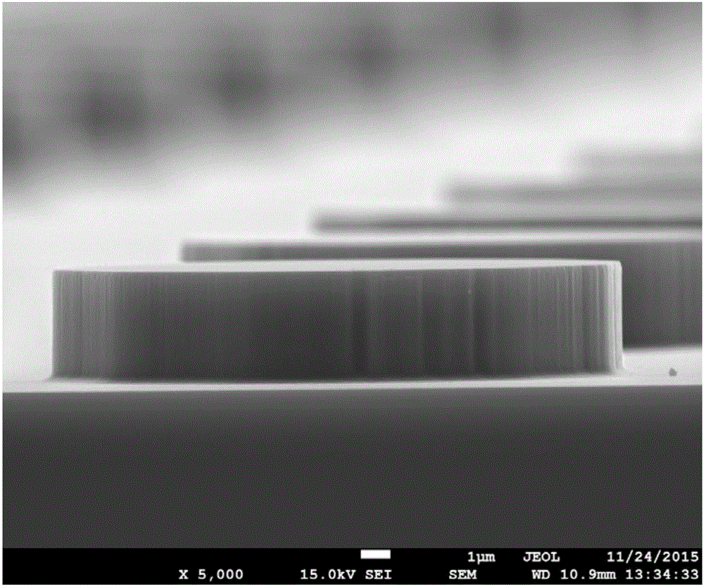
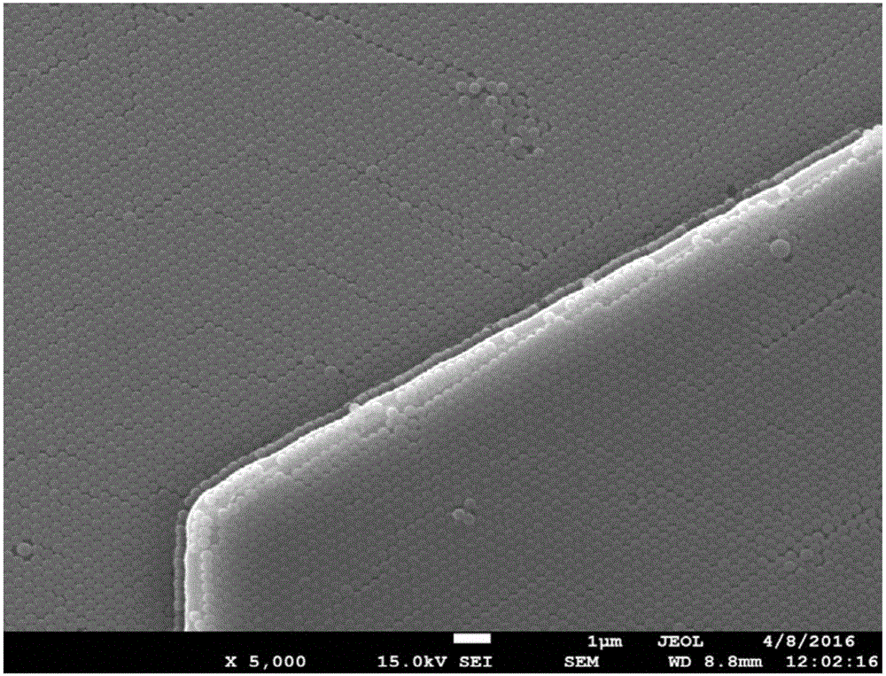
[0030] (4) Prepare the mask plate required for the ultraviolet lithography, which contains periodic structures of square, circular, hexagonal and irregular shapes with different sizes from 4 μm to 60 μm.
[0031] (5) Put the processed silicon wafers into the homogenizer for homogenization. AZ5214e photoresist is used. The homogenization parameters are 500 rpm for the first stage, 5 seconds of rotation, and 6000 revolutions for the second stage. / minute,...
PUM
 Abstract
Description
Claims
Application Information
 - R&D Engineer
- R&D Manager
- IP Professional
- Industry Leading Data Capabilities
- Powerful AI technology
- Patent DNA Extraction
Browse by: Latest US Patents, China's latest patents, Technical Efficacy Thesaurus, Application Domain, Technology Topic.
© 2024 PatSnap. All rights reserved.Legal|Privacy policy|Modern Slavery Act Transparency Statement|Sitemap