Superlattice graded buffer layer transmissive AlGaN ultraviolet cathode and preparation method therefor
A technology of composition gradient and buffer layer, applied in the direction of semiconductor devices, electrical components, circuits, etc., can solve the problem that the photoemission performance of the transmissive AlGaN ultraviolet photocathode cannot be effectively improved, the short-wave response characteristics of the transmissive cathode are affected, and the buffer layer is reduced. Buffer layer and other issues, to achieve the effect of improving photoemission quantum efficiency, increasing the number of electrons escaping, and reducing lattice mismatch
- Summary
- Abstract
- Description
- Claims
- Application Information
AI Technical Summary
Problems solved by technology
Method used
Image
Examples
preparation example Construction
[0015] The preparation method of the transmissive AlGaN ultraviolet photocathode of the superlattice gradient component gradient structure buffer layer of the present invention, the steps are as follows:
[0016] In step 1, the substrate layer 1 of the transmissive cathode is prepared with double-polished sapphire.
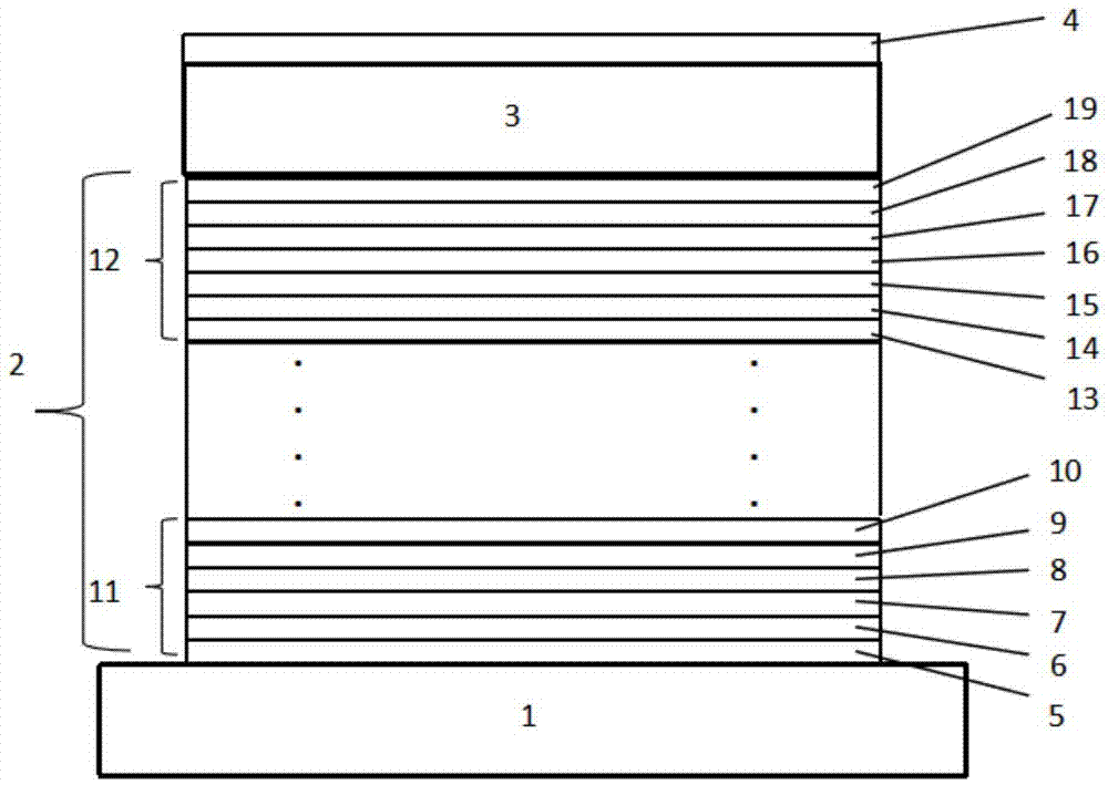
[0017]Step 2, using molecular beam epitaxy to grow 8-15 composition graded layers 11 on the sapphire substrate, and then growing a transition layer 12 on the surface of the uppermost composition graded layer 11, consisting of 8-15 composition graded layers 11 cyclic stacking and a transition layer 12 composed of superlattice gradient composition graded p-type Al x Ga 1-x N buffer layer 2. Each composition graded layer 11 is composed of 5-8 different compositions of Al from bottom to top x Ga 1-x Composed of N thin layers, where 0y Ga 1-y Consisting of N thin layers, where 0y Ga 1-y N emitter layer 3 is the same.
[0018] Step 3, use the molecular beam epita...
Embodiment
[0022] like figure 1 As shown, the transmissive AlGaN ultraviolet photocathode of the superlattice gradient composition buffer layer of the present invention, the cathode is composed of a cathode transmissive substrate layer 1 (made of sapphire), a superlattice gradient composition gradient from bottom to top Structure Ga 1-x al x N buffer layer 2, p-type doped Ga 0.6 al 0.4 The N emission layer 3 and the Cs or Cs / O (cesium oxygen co-activation) active layer 4 are composed.
[0023] The superlattice graded composition buffer layer is composed of 8-15 composition graded layers 11 stacked cyclically and the contact layer 12 with the emission layer, in which the six thin layer components of the composition graded layer are: AlN5, Al 0.9 Ga 0.1 N6, Al 0.8 Ga 0.2 N7, Al 0.7 Ga 0.3 N8, Al 0.8 Ga 0.2 N9 and Al 0.9 Ga 0.1 N10, the components of the seven thin layers of the transition layer are: AlN13, Al 0.9 Ga 0.1 N14, Al 0.8 Ga 0.2 N15, Al 0.7 Ga 0.3 N16, Al 0.6...
PUM
| Property | Measurement | Unit |
|---|---|---|
| Thickness | aaaaa | aaaaa |
| Thickness | aaaaa | aaaaa |
| Thickness | aaaaa | aaaaa |
Abstract
Description
Claims
Application Information

