Method for preparing beta-silicon carbide film

A technology of silicon carbide and thin film, which is applied in the manufacture of semiconductor/solid-state devices, electrical components, circuits, etc., can solve the problems of difficult application of silicon carbide materials, reduce lattice defects, improve heat dissipation performance and service life, and low cost Effect

Inactive Publication Date: 2013-10-09
DALIAN UNIV OF TECH
View PDF6 Cites 9 Cited by
  • Summary
  • Abstract
  • Description
  • Claims
  • Application Information

AI Technical Summary

Problems solved by technology

However, due to the strong adhesion between silicon carbide film material and silicon (Si) substrate, it is difficult to peel off from the substrate, so the application of silicon carbide material in this field has become a big problem

Method used


Image

  • Method for preparing beta-silicon carbide film
  • Method for preparing beta-silicon carbide film
  • Method for preparing beta-silicon carbide film

Examples


Embodiment 1

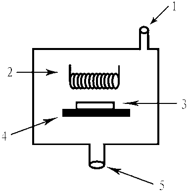
[0034] The preparation method of a kind of β-silicon carbide film of the present invention comprises the following steps:

[0035] Step 1: Divide the 0.5×0.5 mm 2 The graphite substrate with high electrical conductivity and thermal conductivity was cleaned with acetone, absolute ethanol and deionized water for 10 minutes in sequence, and then the substrate was blown dry with high-purity nitrogen.

[0036] Step 2: Optimizing experimental parameters such as silane concentration, reaction system gas pressure, and substrate temperature; the silicon source is silane with a concentration of 10%, the gas flow rate is 0.5 sccm, the gas pressure of the reaction system is 40Pa, and the substrate temperature is 300°C.

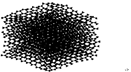
[0037] Step 3: Grow a layer of silicon carbide (SiC) film (100 nm) on the pre-cleaned graphite substrate using HFCVD technology, wherein the temperature of the hot tungsten wire is 2000 °C.

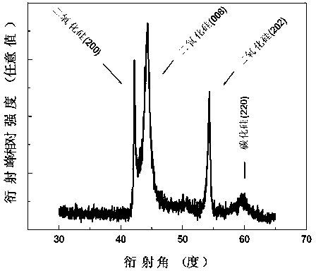
[0038] Step 4: The above-mentioned SiC film is annealed in argon at 500° C. for...

Embodiment 2

[0041] The preparation method of a kind of β-silicon carbide film of the present invention comprises the following steps:

[0042] Step 1: Place 0.5×0.5 cm 2 The graphite substrate with high electrical conductivity and thermal conductivity was cleaned with acetone, absolute ethanol and deionized water for 10 minutes in sequence, and then the substrate was blown dry with high-purity nitrogen.

[0043] Step 2: Optimizing experimental parameters such as silane concentration, reaction system gas pressure, and substrate temperature; the silicon source is silane with a concentration of 10%, the gas flow rate is 0.5 sccm, the gas pressure of the reaction system is 40Pa, and the substrate temperature is 300°C.

[0044] Step 3: Grow a layer of silicon carbide (SiC) film (100 nm) on the pre-cleaned graphite substrate using hot wire chemical vapor deposition (HFCVD), where the temperature of the hot tungsten wire is 2000 °C.

[0045] Step 4: The above-mentioned SiC thin film is annealed i...

Embodiment 3

[0048] The preparation method of a kind of β-silicon carbide film of the present invention comprises the following steps:

[0049] Step 1: Place 0.5×0.5 cm 2 The graphite substrate with high electrical conductivity and thermal conductivity was cleaned with acetone, absolute ethanol and deionized water for 10 minutes in sequence, and then the substrate was blown dry with high-purity nitrogen.

[0050] Step 2: Optimizing experimental parameters such as silane concentration, reaction system gas pressure, and substrate temperature; the silicon source is 10% silane, the gas flow rate is 0.5 sccm, the gas pressure of the reaction system is 40Pa, and the substrate temperature is 300°C.

[0051] Step 3: Grow a layer of silicon carbide (SiC) film (100 nm) on the pre-cleaned graphite substrate using hot wire chemical vapor deposition (HFCVD), where the temperature of the hot tungsten wire is 2000 °C.

[0052] Step 4: The above SiC film is annealed in argon at 700° C. for 30 minutes to ...


PUM


Abstract

The invention relates to the technical field of semiconductor materials, and discloses a method for preparing a beta-silicon carbide film. The method comprises the following steps: silane is used as a silicon source, hydrogen is used as a diluent gas and a carrier gas for the silicon source, graphite is used as a substrate and a carbon source, the beta-silicon carbide film is prepared on the graphite substrate through a hot filament chemical vapor deposition method, the prepared beta-silicon carbide film is subjected to follow-up annealing treatment in an inert gas, and a finished beta-silicon carbide film is obtained further through micromechanical cleavage. According to the novel method, the beta-silicon carbide film is prepared on the graphite substrate, namely the beta-silicon carbide film is prepared on the graphite substrate which has high electric conductivity and heat conductivity, lattice imperfection inside the film is reduced, the crystalline quality of the film is greatly improved, therefore, the heat dispersion performance of a silicon carbide-based electronic (photoelectronic) high-power device is improved, and the service life of the silicon carbide-based electronic (photoelectronic) high-power device is prolonged; the cleavage of a silicon carbide film material and the graphite substrate is easy to realize through the micromechanical cleavage and other methods, and the method for preparing the beta-silicon carbide film is simple, practicable and low in cost.

Description

technical field [0001] The invention relates to the technical field of semiconductor materials, in particular to a method for preparing a β-silicon carbide film on a graphite substrate. Background technique [0002] Silicon carbide (SiC) thin films have unique characteristics such as large band gap, high breakdown electric field, high thermal conductivity, high electron saturation drift velocity, small dielectric constant, strong radiation resistance, and good chemical stability. It is favored in high-frequency, high-power, high-temperature electronic devices and optoelectronic devices, and is known as one of the most promising third-generation semiconductor materials. However, silicon carbide materials have many crystal forms and are very difficult to prepare. For example, β-silicon carbide has a cubic crystal structure, similar to diamonds, and needs to be produced at temperatures below 2000 °C. [0003] In the application of silicon carbide-based devices, the heat dissip...

Claims


Application Information

Patent Timeline
Patent Type & Authority Applications(China)
IPC IPC(8): H01L21/205
Inventor 边继明张志坤毕凯峰刘艳红刘维峰秦福文
Owner DALIAN UNIV OF TECH
Why Eureka
Try Eureka