Integrated technology of reducing CMOS image sensor white pixels

An image sensor and white pixel technology, which is applied in the manufacture of electric solid-state devices, semiconductor devices, and semiconductor/solid-state devices, etc., can solve the problems of rising white pixels and difficult process control, and achieves reduction of white pixels and lattice defects. Effect

Active Publication Date: 2015-12-23
SHANGHAI HUALI MICROELECTRONICS CORP
View PDF6 Cites 9 Cited by
  • Summary
  • Abstract
  • Description
  • Claims
  • Application Information

AI Technical Summary

Problems solved by technology

Although these measures can reduce the number of white pixels, the process control is very difficult, because a very low concentration of metal contamination can cause a sharp increase in white pixels

Method used


Image

  • Integrated technology of reducing CMOS image sensor white pixels
  • Integrated technology of reducing CMOS image sensor white pixels
  • Integrated technology of reducing CMOS image sensor white pixels

Examples


Embodiment Construction

[0028] The specific embodiment of the present invention will be further described in detail below in conjunction with the accompanying drawings.

[0029] It should be noted that in the following specific embodiments, when describing the embodiments of the present invention in detail, in order to clearly show the present invention for the convenience of description, the structures in the drawings are not drawn according to the general scale, and partial Enlargement, deformation and simplified processing, therefore, should be avoided as limiting the understanding of the present invention.

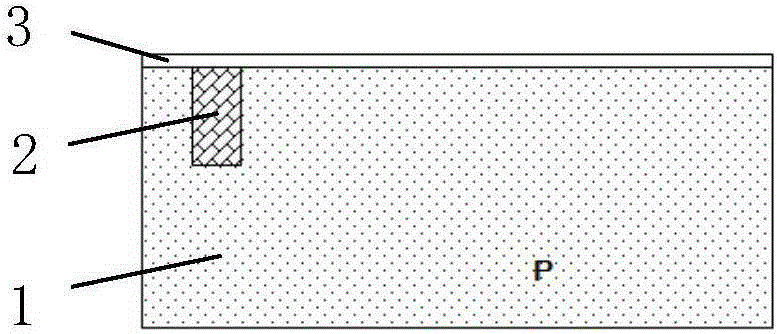
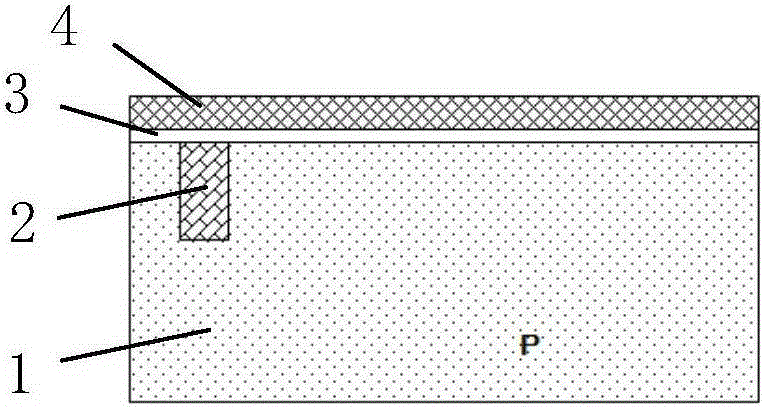
[0030] In the following specific embodiments of the present invention, please refer to figure 1 , figure 1 It is a flowchart of an integration process for reducing white pixels of a CMOS image sensor in the present invention; at the same time, please refer to Figure 2 to Figure 8 , Figure 2 to Figure 8 is a preferred embodiment of the present invention according to figure 1 Schematic di...


PUM


Abstract

The present invention discloses an integrated technology of reducing CMOS image sensor white pixels. The integrated technology comprises the steps of forming the shallow trench isolation in a matrix; growing a pad oxide layer and a silicon nitride barrier layer orderly on the surface of the matrix; coating a photoresist, taking the graphical photoresist as the barrier layer, and penetrating the silicon nitride barrier layer to carry out the ion implantation on the matrix to form a photodiode and an isolation area around the photodiode in the matrix; removing the silicon nitride barrier layer and the pad oxide layer, and then growing a gate oxide layer and a polycrystalline silicon layer; forming a polycrystalline silicon transmission gate and a side wall, and carrying out the shallow-layer ion implantation; forming an interlayer dielectric and a metal layer. The silicon nitride barrier layer can block the ion implantation, especially can block the metal impurities introduced by the metal elements volatilized by the electronic shower during a high energy ion implantation process, at the same time, can reduce the crystal lattice defects caused by an arc effect when the ions are implanted in a shallow-layer area, thereby reducing the white pixels effectively.

Description

technical field [0001] The invention relates to the technical field of semiconductor integrated circuit manufacturing, and more particularly, relates to an integration process for reducing white pixels of a CMOS image sensor. Background technique [0002] In recent years, with the rapid development of mobile networks, mobile smart terminals have been widely popularized and constantly updated. The image sensor, which is the "eye" of the mobile terminal, is also following the market demand and constantly improving its performance. [0003] The future direction of image sensor development is high pixel, low power consumption, and high image quality. High pixel count and low power consumption require continuous reduction in pixel size. However, as the pixel size shrinks, the quality of the pixel drops dramatically, especially the quantum efficiency and noise. Quantum efficiency can be compensated by high-energy ion implantation to elongate the photodiode depth, but noise redu...

Claims


Application Information

Patent Timeline
Patent Type & Authority Applications(China)
IPC IPC(8): H01L21/8238H01L27/146H01L21/31H01L21/265
CPCH01L21/0217H01L21/265H01L21/8238H01L27/14645H01L27/14687
Inventor 范晓陈昊瑜王奇伟
Owner SHANGHAI HUALI MICROELECTRONICS CORP
Why Eureka
Try Eureka