Manufacturing method of N type all-aluminum back emitter solar cell and solar cell prepared by the same

A technology of a solar cell and a manufacturing method, applied in the field of solar cells, can solve the problems of small effective area of ​​PN junction, easy damage of PN junction, lower battery efficiency, etc., so as to reduce the loss of open-circuit voltage and short-circuit current, and increase the PN junction. Area, composite center reduction effect

Inactive Publication Date: 2015-08-26
DK ELECTRONICS MATERIALS INC
View PDF3 Cites 9 Cited by
  • Summary
  • Abstract
  • Description
  • Claims
  • Application Information

AI Technical Summary

Problems solved by technology

Aluminum back-emitter solar cells have low process cost, simple operation, and are easy to realize industrialization; however, the cells made by conventional aluminum back-emitter cells are formed during the sintering process, so the back surface The aluminum back emitter 104 is not a full back field, and the PN junction with the back silver electrode 106 is easily damaged, thereby easily forming a leakage current. The existence of this leakage leads to a significant decrease in battery efficiency; in addition, the aluminum back emitter 104 does not cover the positive There is a back side, so that the back side is not an all-aluminum back emitter, and there is no PN junction at the back silver electrode, and the effective area of ​​the PN junction is relatively small, so the efficiency is also low.

Method used


Image

  • Manufacturing method of N type all-aluminum back emitter solar cell and solar cell prepared by the same
  • Manufacturing method of N type all-aluminum back emitter solar cell and solar cell prepared by the same
  • Manufacturing method of N type all-aluminum back emitter solar cell and solar cell prepared by the same

Examples


Embodiment 1

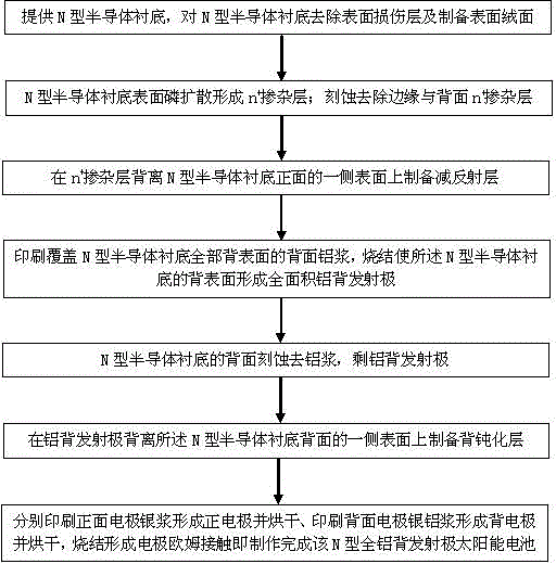
[0053] This embodiment provides a manufacturing method of an N-type aluminum back solar cell, the process flow of the manufacturing method is as follows image 3 As shown, the steps of the production method are as follows:

[0054] (1) Provide a single crystal silicon wafer or a polycrystalline silicon wafer as an N-type semiconductor substrate; remove the surface damage layer and prepare a surface suede on the N-type semiconductor substrate.

[0055] (2) Phosphorus is diffused on the surface of the N-type semiconductor substrate to form n + doped layer, and etch to remove the n on the edge and back + doped layer.

[0056] Usually with POCl 3 Diffusion to form n + doped layer. no + The doped layer is not only formed on the front (front surface) of the N-type semiconductor substrate, but also on the edge and the back; so the edge and back of the N-type semiconductor substrate are de-PSG and etched to remove the n + doped layer.

[0057] It should be noted that the "fr...

Embodiment 2

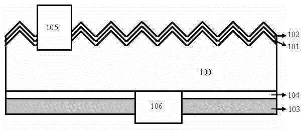
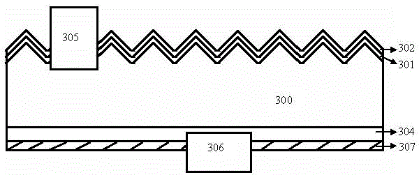
[0077] Based on the first embodiment, this embodiment provides an N-type all-aluminum back-emitter solar cell, such as figure 2As shown, the N-type all-aluminum back-emitter solar cell includes:

[0078] N-type semiconductor substrate 300;

[0079] Covering the n on the front side of the N-type semiconductor substrate 300 + doped layer 301;

[0080] covered in the n + An anti-reflection layer 302 on the surface of the doped layer 301 away from the front side of the N-type semiconductor substrate 300;

[0081] An aluminum back emitter 304 located on the back of the N-type semiconductor substrate 300 and covering the entire back of the N-type semiconductor substrate 300;

[0082] A back passivation layer 307 covering the surface of the aluminum back emitter 304 away from the back side of the N-type semiconductor substrate 300, wherein the back passivation layer 307 has a thickness of 1 nm to 100 nm and is made of aluminum oxide and nitrogen a double-layer structure of a si...


PUM


Abstract

The invention discloses a manufacturing method of an N type all-aluminum back emitter solar cell and a solar cell prepared by the same. The manufacturing method comprises: providing an N type semiconductor substrate, removing a surface damage layer, and preparing a surface pile face; carrying out phosphorus diffusion to form an n<+> doping layer and etching and removing the parts, formed at the edge and the back, of the n<+> doping layer; preparing an antireflection layer at the front side; printing a back aluminium paste and carrying out sintering to form a full-area aluminum back emitter; carrying out etching at the back and removing the aluminium paste and keeping the aluminum back emitter; preparing a back passivation layer at the back; printing a front electrode silver paste and carrying out drying, printing a back electrode silver-aluminium paste and carrying out drying, and carrying out sintering to form electrode ohmic contact. According to the invention, a problem of leak current existence at the boundary of the local back aluminium emitter and the back silver electrode can be solved; the solar cell quality is improved; and the conversion efficiency is improved by increasing the effective area of the PN node. With the back passivation layer, the open-circuit voltage and short-circuit current of the cell are increased. Moreover, the dual-face solar cell can be manufactured, so that the cell energy output is enhanced and the conversion efficiency is improved.

Description

technical field [0001] The invention relates to the technical field of solar cells, in particular to a method for making an N-type all-aluminum back-emitter solar cell that improves the conversion efficiency of a traditional aluminum back-emitter solar cell and the solar cell prepared by the method. Background technique [0002] A solar cell is a semiconductor device that converts the sun's light energy directly into electrical energy. Because it is a green product, does not cause environmental pollution, and uses renewable resources, solar cells have broad prospects for development in today's energy shortage situation. [0003] There are various types of solar cells, among which, N-type solar cells have attracted more and more attention from people in the industry because of their high conversion efficiency. The "boron-oxygen pair" of the P-type silicon substrate will cause the problem of efficiency attenuation, but the use of the N-type silicon substrate does not have thi...

Claims


Application Information

Patent Timeline
Patent Type & Authority Applications(China)
IPC IPC(8): H01L31/18H01L31/0352H01L31/0216H01L31/068
CPCH01L31/02167H01L31/035272H01L31/0682H01L31/0684H01L31/1804H01L31/182Y02E10/546Y02E10/547Y02P70/50
Inventor 史卫利朱亮
Owner DK ELECTRONICS MATERIALS INC
Why Eureka
Try Eureka