Power distribution network design method based on decoupling region of decoupling capacitor
A power distribution network, decoupling capacitor technology, applied in CAD circuit design, calculation, electrical digital data processing and other directions, can solve the problems of failed decoupling design, neglect, voltage distribution is not a constant value, etc., to achieve decoupling radius accuracy High, reduce design cost, shorten the effect of development cycle
Active Publication Date: 2016-09-21
XIDIAN UNIV
View PDF3 Cites 16 Cited by
- Summary
- Abstract
- Description
- Claims
- Application Information
AI Technical Summary
Problems solved by technology
The disadvantage of this method is that the calculation efficiency gradually decreases with the increase of the number of decoupling capacitors
However, the disadvantage of this method is that the power ground plane in the power distribution network is equivalent to a lumped capacitor for decoupling design, and the installation position information of the decoupling capacitor cannot be obtained, ignoring the actual circuit design. The effect of parasitic inductance on the ground plane on the decoupling effect, which may lead to a failed decoupling design
The disadvantage of this method is that the voltage distribution of the power ground plane in the actual circuit is not a constant value, and this assumption seriously affects the reliability of the calculation results
Method used
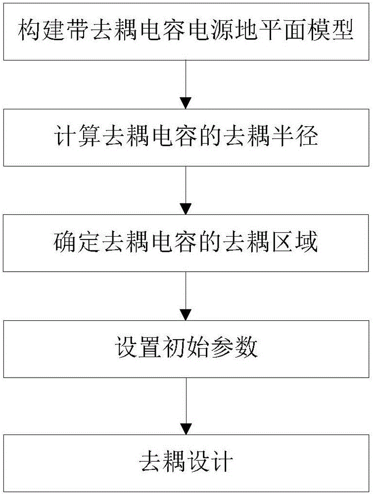
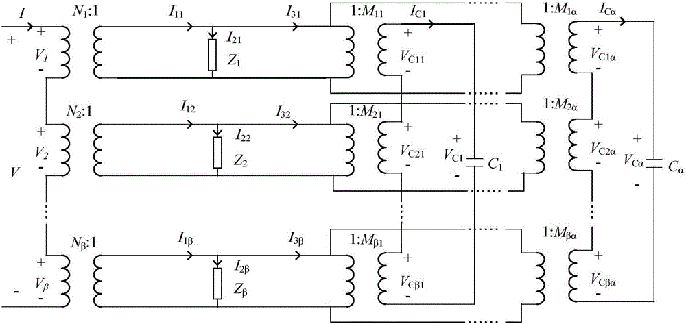
View moreImage
Smart ImageViewing Examples
Examples
Embodiment 1
[0122] 电源地平面的长度为60毫米,宽度为40毫米,平面间隔为0.1毫米,填充介质的介电常数为4.4,介质的损耗角正切是0.02。输入输出端口P0在电源地平面上的位置为(36mm,23mm),目标阻抗设置为0.5Ohm,去耦设计频率为10MHz到1.5GHz,去耦电容库如表2所示。
[0123] 表2.去耦电容库参数表
[0124]
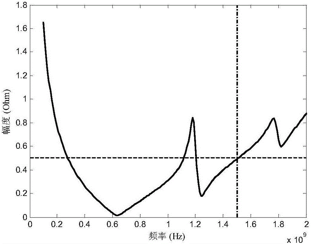
[0125] 基于以上参数,利用本发明的实现步骤,通过MATLAB 2013软件对本发明提出的电源分配网络去耦设计方法进行仿真,选择的去耦电容,电容的去耦半径,去耦电容的安装位置如表3所示。仿真结果如 image 3 as shown, image 3 中横坐标表示频率,单位为赫兹,纵坐标表示阻抗值,单位为欧姆。 image 3 中以实线标示的曲线是电源地平面上添加表3中的去耦电容后输入输出端口P0的阻抗,以虚线标示的直线是目标阻抗,以点划线标示的直线是去耦设计截止目标 frequency. Depend on image 3 可以看出,在去耦设计频率范围内输入输出端口P0的阻抗曲线位于目标阻抗直线的下方,说明在去耦设计频率范围内输入输出端口P0的阻抗小于目标阻抗,证明本发明方法可以正确选择电源分配网络设计时去耦设计所需的去耦电容器及去耦电容的安装位置。
[0126] 表3 选用的去耦电容和去耦电容的安装位置表
[0127]
Login to View More PUM
 Abstract
The invention discloses a power distribution network design method based on a decoupling region of a decoupling capacitor. The power distribution network design method comprises the steps of: firstly, based on a resonant cavity model, modeling a power ground plane with decoupling capacitors; based on the modeling method, calculating out transverse and longitudinal decoupling radii of the decoupling capacitors; according to a frequency point corresponding to the maximum amplitude of an impedance of an input output port, selecting the required decoupling capacitor, and according to the transverse and longitudinal decoupling radii of the decoupling capacitor, selecting an installation position of the decoupling capacitor; and finally, drawing an impedance curve of a power distribution network. According to the invention, the problem that in the power distribution network design, the installation position of the decoupling capacitor cannot be obtained is solved; a rapid, simple and convenient method is provided for selection and placement of the decoupling capacitor in the power distribution network, and reliable guidance is provided for power integrity design in the practical engineering.
Description
technical field [0001] The invention belongs to the field of electronic technology, and further relates to a design method of a power distribution network based on a decoupling capacitor decoupling area in the field of high-speed circuit power distribution technology. The invention can be applied to the design of a power distribution network, and provides a decoupling design scheme including capacitor types and installation positions. Background technique [0002] With the continuous improvement of clock frequency and integration of high-speed digital circuits, the power supply noise generated in the power distribution network seriously limits the improvement of circuit performance. The power ground plane plays a very important role in high frequency digital integrated circuits. In the past, the power ground plane was modeled using lumped components, but the power ground plane will resonate at high frequencies, showing distribution characteristics, and the lumped model cann...
Claims
Login to View More Application Information
Patent Timeline
 Patent Type & Authority Applications(China)
IPC IPC(8): G06F17/50
CPCG06F30/39Y02E60/00
Inventor 路建民王君李先锐初秀琴
Owner XIDIAN UNIV


