Composite structure used for silicon material surface and application of composite structure

A composite structure and silicon material technology, applied in semiconductor devices, electrical components, nanotechnology, etc., can solve the problem of low light absorption rate of silicon solar cells, and achieve the goal of eliminating disadvantages, enhancing light absorption rate, and reducing light absorption rate fluctuating effect

Inactive Publication Date: 2016-09-28
HUAZHONG UNIV OF SCI & TECH
View PDF3 Cites 4 Cited by
  • Summary
  • Abstract
  • Description
  • Claims
  • Application Information

AI Technical Summary

Problems solved by technology

[0005] In view of the above defects or improvement needs of the prior art, the object of the present invention is to provide a composite structure for the surface of silicon materials and its application, wherein by improving the key shape parameters constituting the composite structure, it is different from the prior art Compared with silicon solar cells, it can effectively solve the problem of low light absorption rate, and the composite structure can reduce the preparation cost of the nanowire structure and improve the overall stability of the composite structure; in addition, by adjusting the internal grating structure and nanowire structure of the composite structure The arrangement and composition of the array can regulate the light absorptivity on the surface of silicon solar cells and reduce the fluctuation of light absorptivity caused by different light bands

Method used


Image

  • Composite structure used for silicon material surface and application of composite structure
  • Composite structure used for silicon material surface and application of composite structure
  • Composite structure used for silicon material surface and application of composite structure

Examples


Embodiment Construction

[0032] In order to make the objectives, technical solutions and advantages of the present invention clearer, the following further describes the present invention in detail with reference to the accompanying drawings and embodiments. It should be understood that the specific embodiments described herein are only used to explain the present invention, but not to limit the present invention. In addition, the technical features involved in the various embodiments of the present invention described below can be combined with each other as long as they do not conflict with each other.

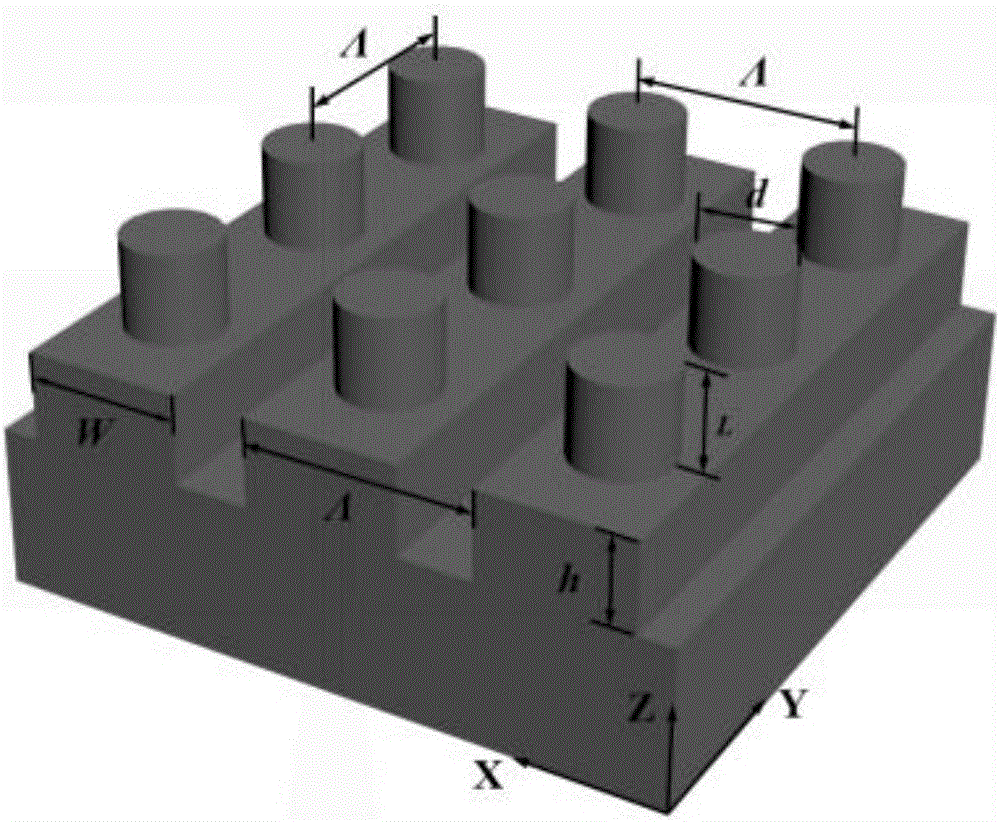
[0033] Such as figure 1 As shown, the grating-nanowire composite structure of the present invention is arranged on a silicon substrate, which can be regarded as semi-infinitely thick in the Z direction (when the silicon substrate is single crystal silicon, the Z direction can be parallel to the silicon single crystal). The c-axis direction of the unit cell), periodic one-dimensional gratings are unifor...


PUM

PropertyMeasurementUnit
Widthaaaaaaaaaa
Heightaaaaaaaaaa
Diameteraaaaaaaaaa

Abstract

The invention discloses a composite structure used for silicon material surface and application of the composite structure. The composite structure includes a grating structure and nanowire arrays. The grating structure includes a plurality of cuboids arranged in parallel periodically. The distance between each two adjacent cuboids is fixed. The nanowire arrays are a plurality of cylinders arranged periodically and disposed on the top faces of the cuboids of the grating structures. The distance between the central axes of two adjacent cylinders disposed on the top face of one cuboid is fixed. According to the invention, through improvement on key shape parameters of the composite structure, light absorption efficiency of a silicon solar cell can be improved, manufacture cost can be reduced and the integral stability of the composite structure is improved. Besides, through adjusting the arrangement method of the grating structure and the nanowire arrays in the composite structure, the light absorption rate of the surface of the silicon solar cell can be regulated and fluctuation of light absorption rate due to difference of light wavebands is reduced.

Description

Technical field [0001] The invention belongs to the technical field of solar cell anti-reflection system design, and more specifically, relates to a composite structure used on the surface of silicon material and its application. The composite structure is suitable for photovoltaic power generation systems, especially silicon solar cells, and can improve solar cells. The light absorption rate improves the photoelectric conversion efficiency of solar cells. Background technique [0002] Solar cells are a device that can convert solar energy into electrical energy. With the emergence of energy crisis and environmental problems, photovoltaic power generation technology has become more and more important. The application of solar cells can be traced back to the 1950s, and many scholars at home and abroad have conducted research on them. After more than half a century of development, there are many types of solar cells, and their absorption rate and conversion rate have also been gre...

Claims


Application Information

Patent Timeline
IPC IPC(8): H01L31/0236H01L31/028H01L31/042B82Y20/00
CPCB82Y20/00H01L31/02366H01L31/028H01L31/042Y02E10/547
Inventor 程强贾志浩宋金霖刘杨司梦婷
Owner HUAZHONG UNIV OF SCI & TECH
Why Eureka
Try Eureka