Bio-electricity signal collecting device
A technology of bioelectrical signal and acquisition device, which is applied in the field of transmission and bioelectrical signal detection, can solve the problems of loose cap body, unsafe human body, and high cost, and achieve the effects of simplifying production and processing technology, reducing skin impedance, and prolonging service life
- Summary
- Abstract
- Description
- Claims
- Application Information
AI Technical Summary
Problems solved by technology
Method used
Image
Examples
Embodiment 1
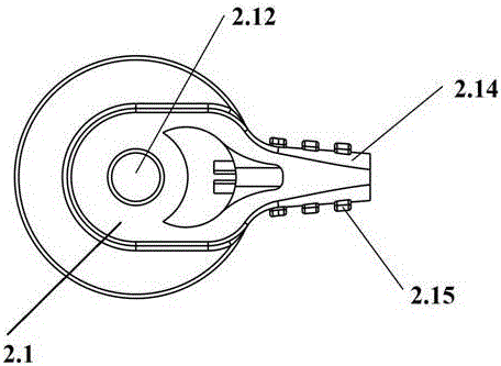
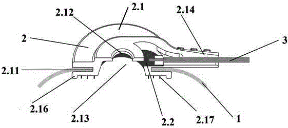
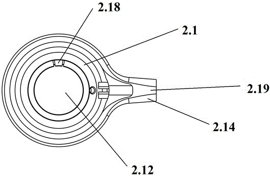
[0036] Example 1 : be a basic embodiment of the present invention. Such as figure 1 As shown, the bioelectrical signal acquisition device includes a support body 1, an electrode 2 installed on the support body 1, and a lead wire 3. The support body 1 has electrode positioning holes, and the electrode 2 includes a fixing ring. 2.1, the middle part of the fixed ring 2.1 has a conductive glue cavity 2.13 with both ends open and connected; the inner wall of the conductive glue cavity 2.13 is provided with an electrode sensing layer 2.2, and the electrode sensing layer 2.2 is a gap 2.18 Ring surface, the electrode sensing layer 2.2 is connected to the lead wire 3; the outer cylindrical surface of the fixing ring 2.1 has a fixing groove 2.11, which is used to embed the periphery of the electrode positioning hole to fix the electrode 2 and the support Body 1, the integrated design of the present invention, the electrode as a whole is directly fixed on the cap body without install...
Embodiment 2
[0037] Example 2 : be a further embodiment of the present invention. The difference from Example 1 is that the inner wall of the conductive glue cavity 2.13 is a complete annular surface, and the electrode sensing layer 2.2 partially covers the inner wall surface of the conductive glue cavity 2.13, forming an electrode sensing layer 2.2 with a notched annular surface .
Embodiment 3
[0038] Example 3 : be a further embodiment of the present invention. Such as image 3 , Figure 4 As shown, the difference from Example 2 is that the inner wall of the conductive rubber cavity 2.13 is a notched annular surface, and the electrode sensing layer 2.2 covers the entire inner wall surface of the conductive rubber cavity 2.13 to form an electrode with a notched annular surface Sensing layer 2.2.
PUM
 Abstract
Description
Claims
Application Information


