Microstrip nanometer film microwave electromagnetic parameter testing apparatus

A nano-film, electromagnetic parameter technology, applied in measuring devices, measuring electrical variables, measuring resistance / reactance / impedance and other directions, can solve the problems of difficult processing, low sensitivity, complex structure, etc., to achieve the effect of easy operation

Inactive Publication Date: 2016-10-12
XIAMEN UNIV
View PDF5 Cites 11 Cited by
  • Summary
  • Abstract
  • Description
  • Claims
  • Application Information

AI Technical Summary

Problems solved by technology

Although the resonant cavity method has high test accuracy and simple operation, it can only measure point frequency, and the accuracy and stability of the measurement cannot be guaranteed.
The double-coil method is greatly disturbed by the surrounding electromagnetic field, the error increases, the structure is complex, it is not easy to process, and the sensitivity is low

Method used


Image

  • Microstrip nanometer film microwave electromagnetic parameter testing apparatus
  • Microstrip nanometer film microwave electromagnetic parameter testing apparatus
  • Microstrip nanometer film microwave electromagnetic parameter testing apparatus

Examples


Embodiment Construction

[0018] The present invention will be further described below in conjunction with the accompanying drawings and specific embodiments.

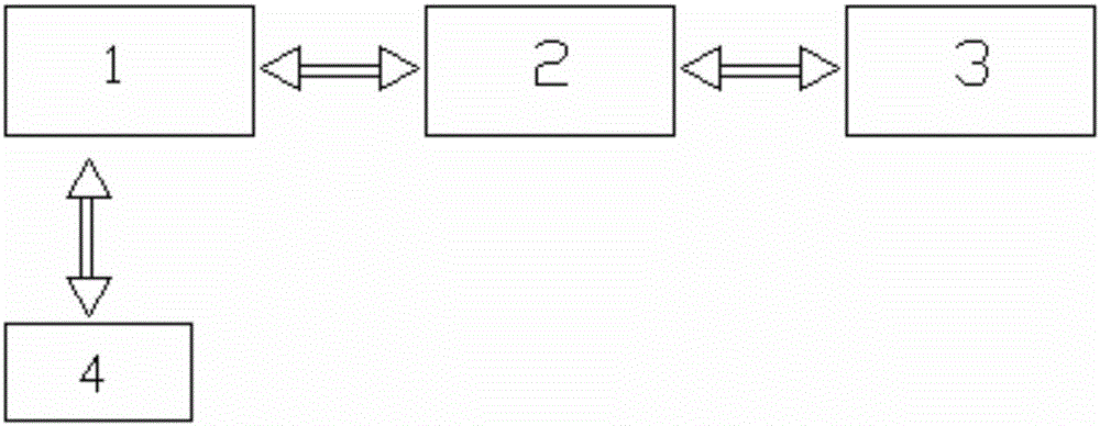
[0019] see figure 1 , the nano film material electromagnetic parameter testing device of the present invention is made up of microwave vector network analyzer 1, GPIB data acquisition card 2, computer 3 and microstrip fixture 4, and one end of the coaxial cable is connected with microwave vector network analyzer 1 The microwave signal port of the coaxial cable, the other end of the coaxial cable is connected to the microstrip fixture 4 through the SMA connector;

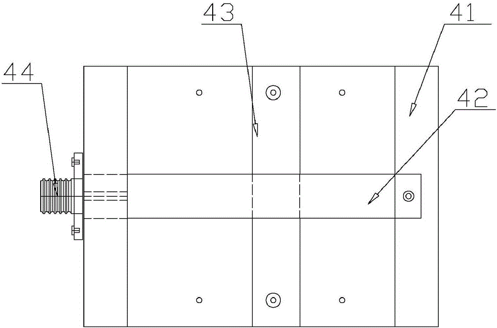
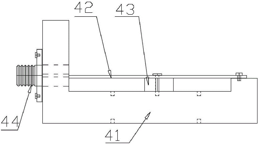
[0020] see Figure 2-7 , The microstrip fixture consists of an L-shaped base 41 , an upper guide strip 42 , an adjustable short circuit 43 , an SMA connector 44 , a shield 45 and a fixed platform 46 . The L-shaped base 41 and the SMA connector 44 are connected and fixed with four screws; the upper guide strip 42 is directly welded to the middle copper core of the SMA connector 44; t...


PUM


Abstract

The invention provides a microstrip nanometer film microwave electromagnetic parameter testing apparatus, which belongs to the technical field of electromagnetic parameter testing. The apparatus is provided with a microstrip clamp, a microwave vector network analyzer, a GPIB data acquisition card, and a computer. The microstrip clamp is composed of an L-shaped base, an upper conduction band, an adjustable short circuit piece, an SMA connector, a shield cover and a fixed platform. One end of the L-shaped base is provided with a circular hole; the other a step. The two ends of the adjustable short circuit piece are provided with grooves. The SMA connector is mounted on the L-shaped base and is connected to the coaxial cable of the microwave vector network analyzer; a nanometer film sample is placed at the center position of the input end and the adjustable short circuit piece. The microstrip clamp is fixed on the fixed platform, and the four corners of the fixed platform are equipped with height adjustable supporting rods. The fixed platform is evenly engraved with a set of horizontal lines marked with scales. Two spring clamp sheets are locked on the fixed platform and are placed on the end face and the face of the microstrip clamp respectively. The apparatus can achieve precise measurement, cause no damage and is convenient to operate.

Description

technical field [0001] The invention relates to a detection of electromagnetic parameters of materials, in particular to a microstrip device for testing nano-film microwave electromagnetic parameters. Background technique [0002] With the rapid development of electronic information technology, the operating frequency and integration of electronic components continue to increase. As one of the key components of electronic components, electromagnetic components must develop in the direction of miniaturization, integration, and high frequency. In recent years, high-frequency electromagnetic thin-film materials have attracted a lot of attention due to their great application potential in the integration and miniaturization of electromagnetic fields, such as thin-film inductors, transformers, and magnetic sensors. Compared with bulk materials, high-frequency electromagnetic thin film materials are more promising as core materials due to their relatively small volume, low coerciv...

Claims


Application Information

Patent Timeline
Patent Type & Authority Applications(China)
IPC IPC(8): G01R27/26G01R33/12
CPCG01R27/2617G01R33/1223
Inventor 肖芬张俊明陈先言李学漪柳清伙刘海
Owner XIAMEN UNIV
Why Eureka
Try Eureka