A kind of semiconductor device and its manufacturing method, electronic device

A manufacturing method and technology for electronic devices, which are applied in semiconductor/solid-state device manufacturing, semiconductor devices, circuits, etc., can solve problems such as TiN loss, content limitation, and main spacer damage.

Active Publication Date: 2019-04-09
SEMICON MFG INT (SHANGHAI) CORP
View PDF3 Cites 0 Cited by
  • Summary
  • Abstract
  • Description
  • Claims
  • Application Information

AI Technical Summary

Problems solved by technology

However, there is still the phenomenon of TiN loss, which is mainly caused by the following two reasons: (1) the normal NiSi cycle cleaning is very strong, and the main spacer will be partially destroyed, especially in the weak area; (2) for Protect metal gate from falling off and PMOS top shoulder, HF content is limited

Method used


Image

  • A kind of semiconductor device and its manufacturing method, electronic device
  • A kind of semiconductor device and its manufacturing method, electronic device
  • A kind of semiconductor device and its manufacturing method, electronic device

Examples


Embodiment 1

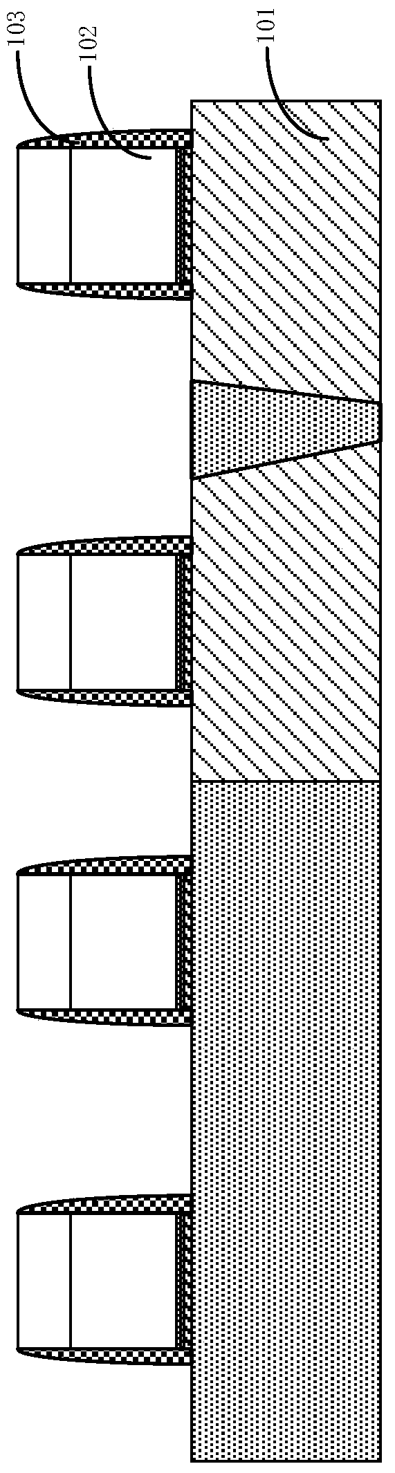
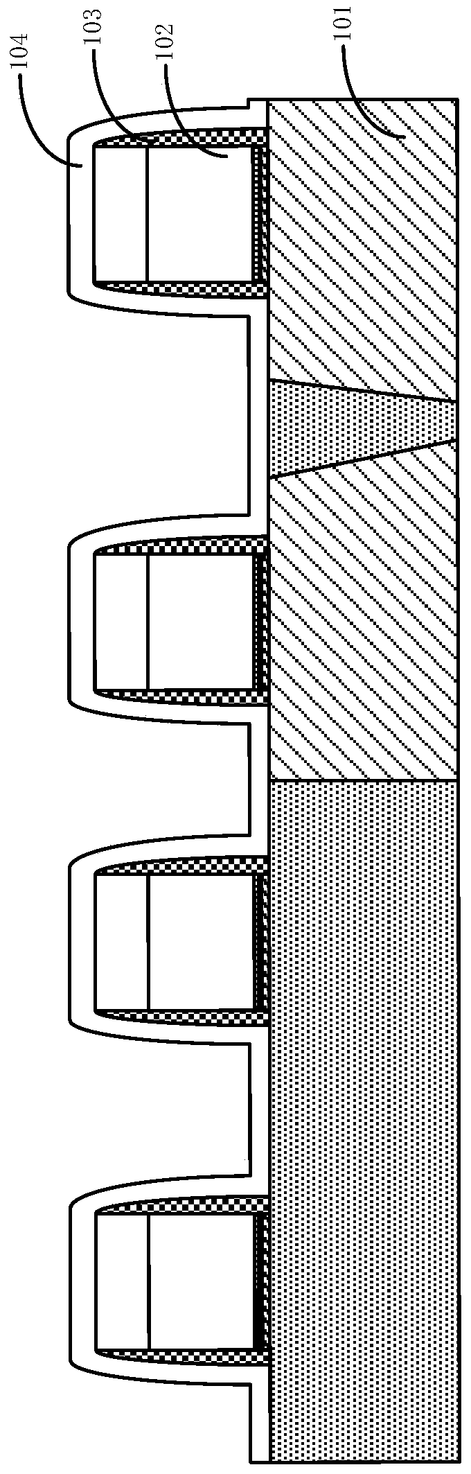
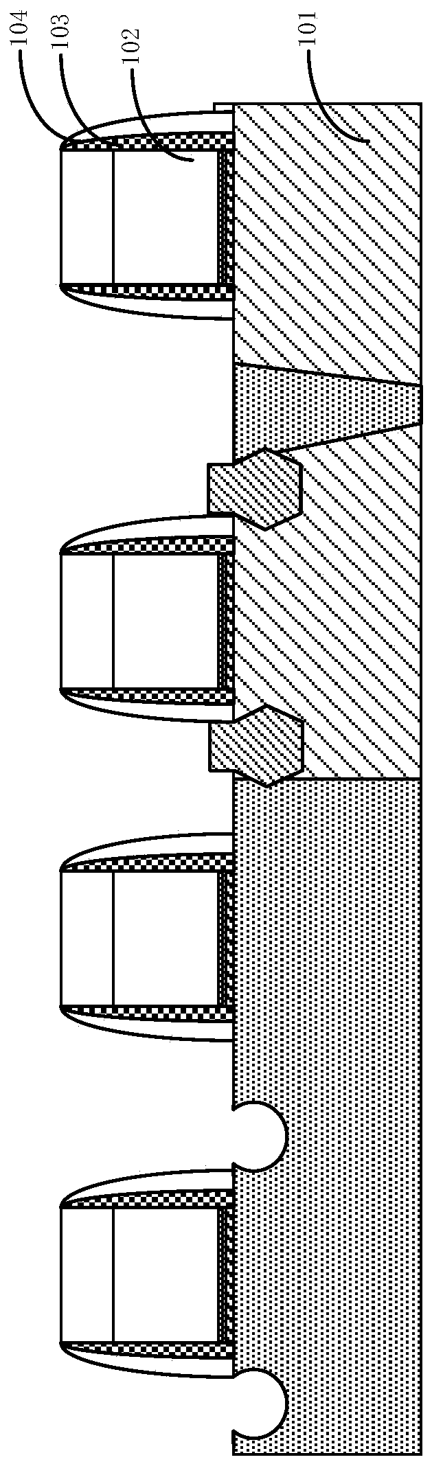
[0069] Below, refer to Figures 3a-3g and Figure 4 The detailed steps of an exemplary method of the method for manufacturing a semiconductor device proposed by the present invention will be described. Among them, 3a-3g are schematic cross-sectional views of graphics formed in the key steps of the manufacturing method of the semiconductor device according to the embodiment of the present invention; Figure 4 It is a flow chart of a method for manufacturing a semiconductor device proposed by an embodiment of the present invention.

[0070] First, step 301 is performed to provide a semiconductor substrate 301, on which a gate including a high-K dielectric layer, a cover layer, a dummy gate and a hard mask layer are respectively formed on the active region and the isolation region of the semiconductor substrate 301. structure, the gate structure includes an NMOS gate structure and a PMOS gate structure.

[0071] As an example, such as Figure 3aAs shown, in this embodiment, t...

Embodiment 2

[0119] The present invention also provides a semiconductor device, which is prepared by the method described in Embodiment 1. No TiN loss occurs in the semiconductor device, metal gate protrusion does not occur after the metal gate is formed, no etch punch-through occurs during dummy gate removal, and metal Al does not occur after the metal gate is formed Diffusion further improves the yield of the semiconductor device.

Embodiment 3

[0121] The present invention also provides an electronic device, including the semiconductor device described in Embodiment 2. Wherein, the semiconductor device is the semiconductor device described in Embodiment 2, or the semiconductor device obtained according to the preparation method described in Embodiment 1.

[0122] The electronic device of this embodiment can be any electronic product or equipment such as mobile phone, tablet computer, notebook computer, netbook, game console, TV set, VCD, DVD, navigator, camera, video recorder, voice recorder, MP3, MP4, PSP, etc. , can also be any intermediate product including the semiconductor device. The electronic device according to the embodiment of the present invention has better performance due to the use of the above-mentioned semiconductor device.


PUM


Abstract

The invention relates to a semiconductor device and a manufacture method thereof, and an electronic device. A substrate at the two sides of a grid structure is etched before a SiGe shielding layer is formed to form recesses at the two sides of the grid structure, the SiGe shielding layer is deposited after the recesses are formed, the SiGe shielding layer uses CVD SiN with a good gap filling capability so that the CVD SiN can be deposited in the sidewall of a groove and partially fill the groove, a gap wall can be formed in the sidewall of the groove in the subsequent etching process of the SiGe shielding layer, the gap wall in the sidewall of the groove can be protected by a main gap wall in subsequent steps, and NiSi is prevented from damage in the cleaning process.

Description

technical field [0001] The present invention relates to the technical field of semiconductors, in particular to a semiconductor device, a manufacturing method thereof, and an electronic device. Background technique [0002] High K metal gate (HKMG) technology and embedded silicon germanium technology (referred to as silicon germanium technology) are important technologies in the semiconductor field. In high-K metal gate technology, high-K dielectric layer and metal gate are the most important components, and thicker high-K dielectric materials are usually used instead of SiO 2 , to obtain lower leakage current. The metal gate comprising the high-K dielectric layer is selected to match the work function layer. TiN is usually formed on top of the high-K dielectric layer to protect the high-K dielectric layer during dummy gate removal in the high-K dielectric layer-then-metal gate process. In addition, TiN is also used in NMOS And / or used as a work function layer in PMOS, Ti...

Claims


Application Information

Patent Timeline
Patent Type & Authority Patents(China)
IPC IPC(8): H01L21/8238H01L21/28
Inventor 倪景华于书坤
Owner SEMICON MFG INT (SHANGHAI) CORP
Why Eureka
Try Eureka