
Film transistor, preparation method thereof and logic circuit
A technology of thin-film transistors and logic circuits, which is applied in the field of semiconductor devices, can solve problems such as high power consumption of circuits, increase of process complexity, and failure of circuit functions, and achieve the effects of low power consumption, reduced process difficulty, and reduced production costs
- Summary
- Abstract
- Description
- Claims
- Application Information
AI Technical Summary
Problems solved by technology
Method used
Image

Examples
Embodiment Construction
[0020] In order to make the objectives, technical solutions, and advantages of the present invention clearer, the specific embodiments of the present invention will be described in detail below with reference to the accompanying drawings. Examples of these preferred embodiments are illustrated in the drawings. The embodiments of the present invention shown in the drawings and described in accordance with the drawings are merely exemplary, and the present invention is not limited to these embodiments.
[0021] Here, it should also be noted that, in order to avoid obscuring the present invention due to unnecessary details, only the structure and / or processing steps closely related to the solution according to the present invention are shown in the drawings, and the Other details not relevant to the present invention.
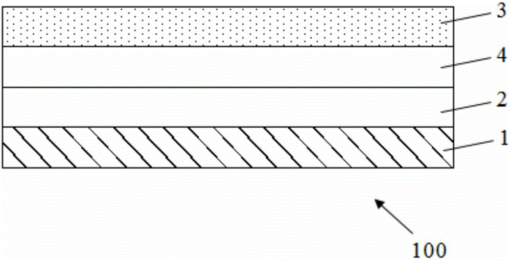
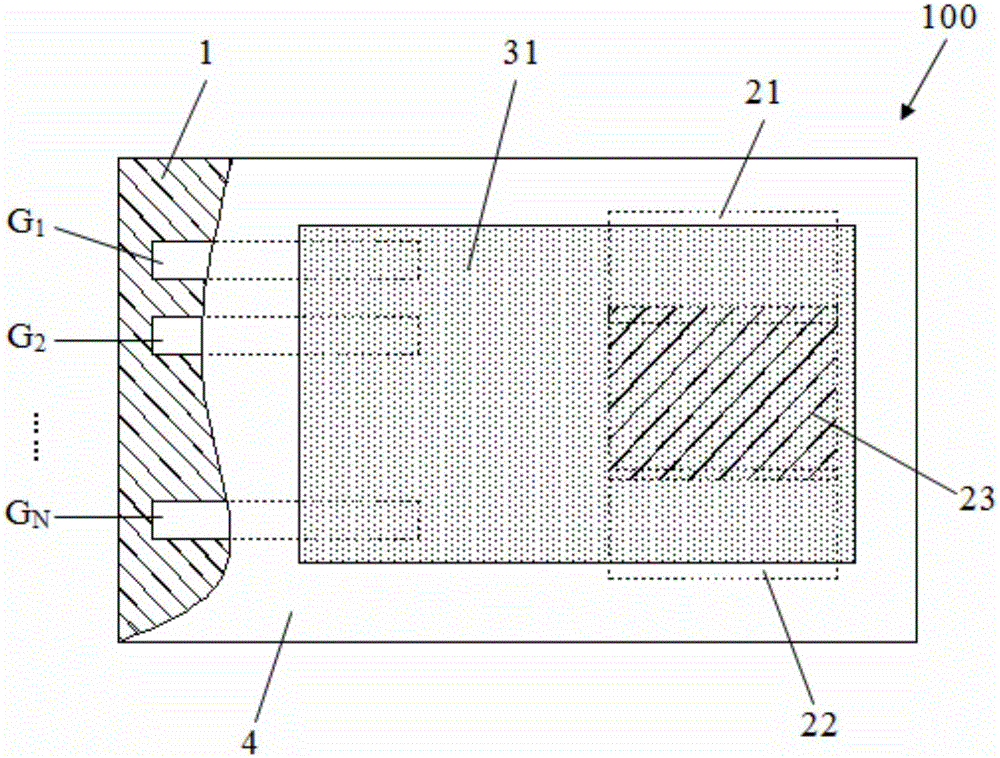
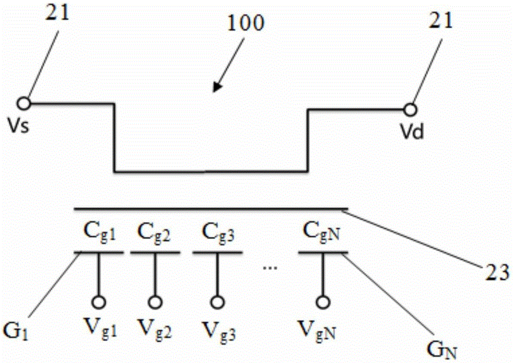
[0022] Refer to figure 1 with figure 2 , This embodiment first provides a thin film transistor, such as figure 1 As shown, the thin film transistor 100 includes a su...
PUM
 Abstract
Description
Claims
Application Information