Wafer level optoelectronic device packages with crosstalk barriers and methods for making the same

A technology of optoelectronic devices and sound barriers, applied in semiconductor/solid-state device manufacturing, electric solid-state devices, electrical components, etc., can solve problems such as high yield, increased manufacturing cost, and loss, and achieve high-yield manufacturing, low cost, and reduced materials The effect of the list

Active Publication Date: 2016-10-26
INTERSIL INC
View PDF2 Cites 6 Cited by
  • Summary
  • Abstract
  • Description
  • Claims
  • Application Information

AI Technical Summary

Problems solved by technology

[0005] see from figure 1 Describing an exemplary prior art optical proximity sensor 102, it can be appreciated that current packaging of optical proximity sensors inv

Method used


Image

  • Wafer level optoelectronic device packages with crosstalk barriers and methods for making the same
  • Wafer level optoelectronic device packages with crosstalk barriers and methods for making the same
  • Wafer level optoelectronic device packages with crosstalk barriers and methods for making the same

Examples


Embodiment Construction

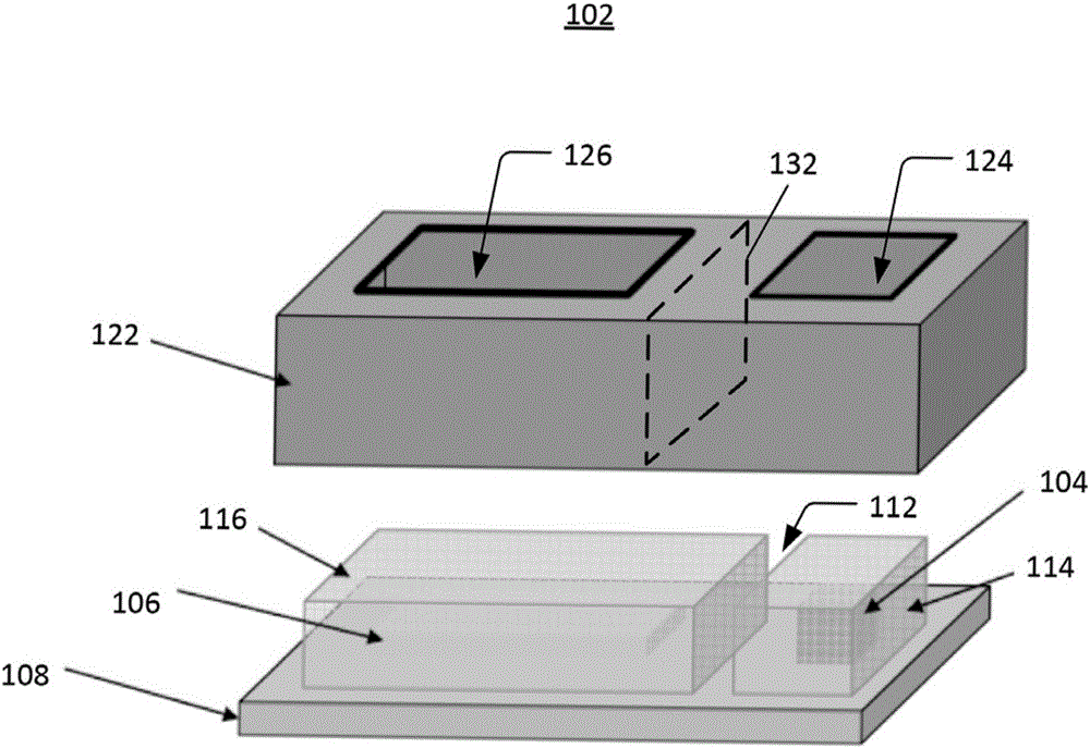
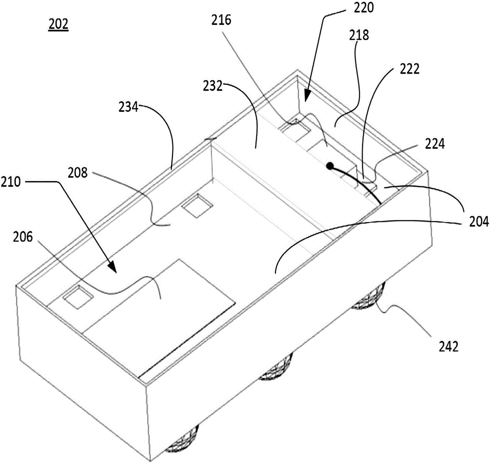
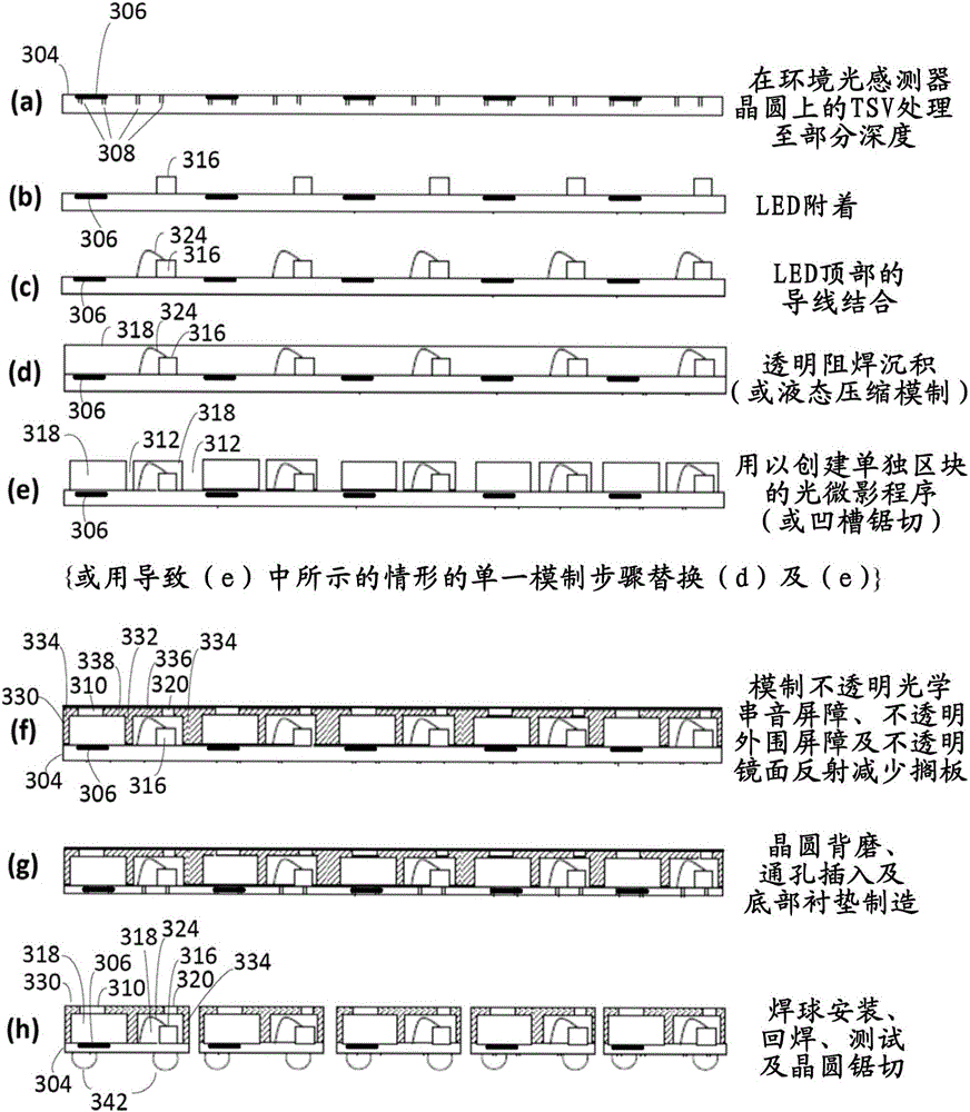
[0032] include section image 3 (a) to image 3 (h) image 3 To illustrate the fabrication of an optoelectronic device (and more particularly, a plurality of such devices) according to certain embodiments. For example, see image 3 The procedure described above can be used to make the above cf. figure 2 An optoelectronic device 202 is depicted.

[0033] Referring to 3( a ), a plurality of photodetector sensor regions 306 are shown formed in a silicon wafer 304 . A through-silicon via (TSV) process is performed to form vias 308 that will provide electrical contacts between components that are connected to the top of the wafer 304 and that will be formed on the bottom of the wafer after backgrinding the wafer (eg, solder balls) between electrical connections. For example, standard TSV processing using plasma etching may be used to form partial depth openings (drilled holes) into wafer 304 . The partial depth TSV process can be performed at the initial or final stages of ...


PUM


Abstract

A method for wafer level fabricating a plurality of optoelectronic devices, starting with a wafer that includes a plurality of light detector sensor regions, includes attaching each of a plurality of light source dies to one of a plurality of bond pads on a top surface of the wafer that includes the plurality of light detector sensor regions. The method also includes attaching, to the wafer, a preformed opaque structure made off-wafer from an opaque material, wherein the preformed opaque structure includes opaque vertical optical barriers. Additionally, solder balls or other electrical connectors are attached to the bottom of the wafer. The wafer is diced to separate the wafer into a plurality of optoelectronic devices, each of which includes at least one of the light detector sensor regions, at least one of the light source dies and at least two of the solder balls or other electrical connectors.

Description

[0001] priority application [0002] This application claims priority to U.S. Patent Application No. 14 / 748,904, filed June 24, 2015, and U.S. Provisional Patent Application No. 62 / 148,569, filed April 16, 2015. technical field [0003] Embodiments of the invention generally relate to wafer-level optoelectronic packaging and methods of manufacturing the same. Background technique [0004] figure 1 Is a perspective view of an exemplary prior art optical proximity sensor 102 including a cover 122 shown removed. The sensor 102 includes a light source die 104 and a light detector die 106 spaced apart from each other and attached to a base substrate 108 , such as a printed circuit board (PCB). The light source die 104 is encapsulated in a transparent epoxy 114 , and the light detector die 106 is individually encapsulated in a transparent epoxy 116 . A gap 112 exists between the transparent epoxy 116 covering the photodetector die 106 and the transparent epoxy 116 covering the ...

Claims


Application Information

Patent Timeline
IPC IPC(8): H01L31/18H01L31/12G01D5/30G01S17/04
CPCG01D5/30H01L31/125H01L31/18G01S7/481H01L2224/48091H01L2224/94H01L2224/97H01L2224/0401H01L2224/0557H01L2224/32145H01L2224/48145H01L2224/73257H01L2224/92247H01L2924/1815G01S17/04H01L2924/00014H01L2224/11H01L2224/85H01L2224/83H01L2224/03H01L25/50H01L21/78
Inventor 斯里·加尼许·A·塔伦玛琳甘
Owner INTERSIL INC
Why Eureka
Try Eureka