Multi-chip joint simulation method based on traditional EDA tool

A co-simulation, multi-chip technology, used in design optimization/simulation, CAD circuit design, special data processing applications, etc., can solve problems such as abnormal circuit operation, avoid manual misoperation, improve reusability, and improve simulation. The effect of efficiency

Inactive Publication Date: 2016-11-09
58TH RES INST OF CETC
View PDF4 Cites 7 Cited by
  • Summary
  • Abstract
  • Description
  • Claims
  • Application Information

AI Technical Summary

Problems solved by technology

[0005] The technical problem to be solved by the present invention is to overcome the existing defects, and provide a method suitable for multi-chip co-simulation on the basis of the existing integrated circuit simulation tools, which is used to verify the ports of the sub-chips in the SiP circuit when they work together. The matching of time and timing can prevent abnormal circuit operation caused by unreasonable circuit parameter design or wrong port connection, and provide a reference for the final SiP design

Method used


Image

  • Multi-chip joint simulation method based on traditional EDA tool
  • Multi-chip joint simulation method based on traditional EDA tool
  • Multi-chip joint simulation method based on traditional EDA tool

Examples


Embodiment Construction

[0021] The embodiments listed in the present invention are only used to help understand the present invention, and should not be interpreted as limiting the protection scope of the present invention. For those of ordinary skill in the art, they can also Improvements and modifications are made to the present invention, and these improvements and modifications also fall within the protection scope of the claims of the present invention.

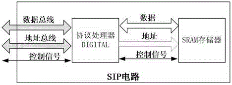
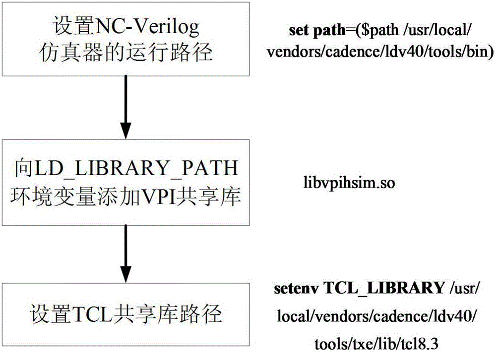
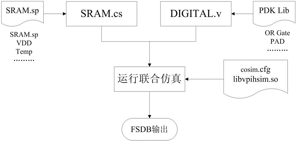
[0022] The present invention is introduced with a SiP circuit composed of protocol processor DIGITAL (digital logic subcircuit) and SRAM memory (analog subcircuit). The composition structure of SiP circuit is as attached figure 1 shown. The simulation tool that the present invention needs is the Verilog simulator NC-Verilog of Cadence Company and the Spice simulator HSIM of Synopsys Company. During co-simulation, the system will call Verilog Program Interface (VPI) or Programmable Language Interface (PLI) to interact with HSIM and NC-Verilog ...


PUM


Abstract

The invention relates to a multi-chip joint simulation method based on a traditional EDA tool. The method includes the steps that a whole SiP circuit is composed of a digital logic sub-circuit and an analog sub-circuit according to circuit functions, wherein a Verilog simulator is adopted in the digital logic sub-circuit, and an HSIM simulator is adopted in the analog sub-circuit or a circuit which is not suitable for being described by Verilog language; it is only needed to apply a unified test vector to the whole SiP circuit during simulation, the Verilog simulator and the HSIM simulator can automatically interact with each other in the whole simulation process, and required simulation intermediate data is transmitted mutually; after simulation, simulation results of all the sub-circuits can be checked by means of a view tool. The method is used for verifying matching performance of ports and time sequences during cooperative work of sub-chips in the SiP circuit, the problem that the circuits work abnormally due to unreasonable design of circuit parameters or port connection errors is prevented, and finally reference is provided for SiP design.

Description

technical field [0001] The invention relates to a chip simulation method, in particular to a multi-chip joint simulation method based on traditional EDA tools. Background technique [0002] The rapid development of electronic information technology has promoted the development of electronic products in the direction of miniaturization, which continuously puts forward requirements for the miniaturization, multi-function, high bandwidth and low power consumption of integrated circuits, and system integration has become more and more important. In order to meet the ever-increasing chip integration level, there are currently two main solutions: one is system-on-chip (SoC) technology, and the other is system-in-package (SiP) technology. SoC technology can integrate high-performance digital circuits and analog circuits in one chip, but this technology has the disadvantages of high cost and complicated process. SiP technology integrates multiple chips and passive devices into one ...

Claims


Application Information

Patent Timeline
Patent Type & Authority Applications(China)
IPC IPC(8): G06F17/50
CPCG06F30/20G06F30/39G06F2113/18G06F2119/18
Inventor 蔡洁明卫博印琴刘士全
Owner 58TH RES INST OF CETC
Why Eureka
Try Eureka