Pixel structure, manufacturing method and display panel

A pixel structure and pixel technology, which is applied in semiconductor/solid-state device manufacturing, semiconductor/solid-state device components, semiconductor devices, etc., can solve the problems of shortening the service life of display devices and increasing the power consumption of display panels, so as to improve light extraction efficiency, reduce power consumption, and prolong service life

Active Publication Date: 2016-11-09
TCL CHINA STAR OPTOELECTRONICS TECH CO LTD
View PDF6 Cites 5 Cited by
  • Summary
  • Abstract
  • Description
  • Claims
  • Application Information

AI Technical Summary

Problems solved by technology

However, limited by the light loss inside the device structure, only about 20% of the output in the device is used, which greatly increases the power consumption of the display panel and shortens the service life of the display device. These have become urgent problems to be solved in the industry

Method used


Image

  • Pixel structure, manufacturing method and display panel
  • Pixel structure, manufacturing method and display panel
  • Pixel structure, manufacturing method and display panel

Examples


Embodiment Construction

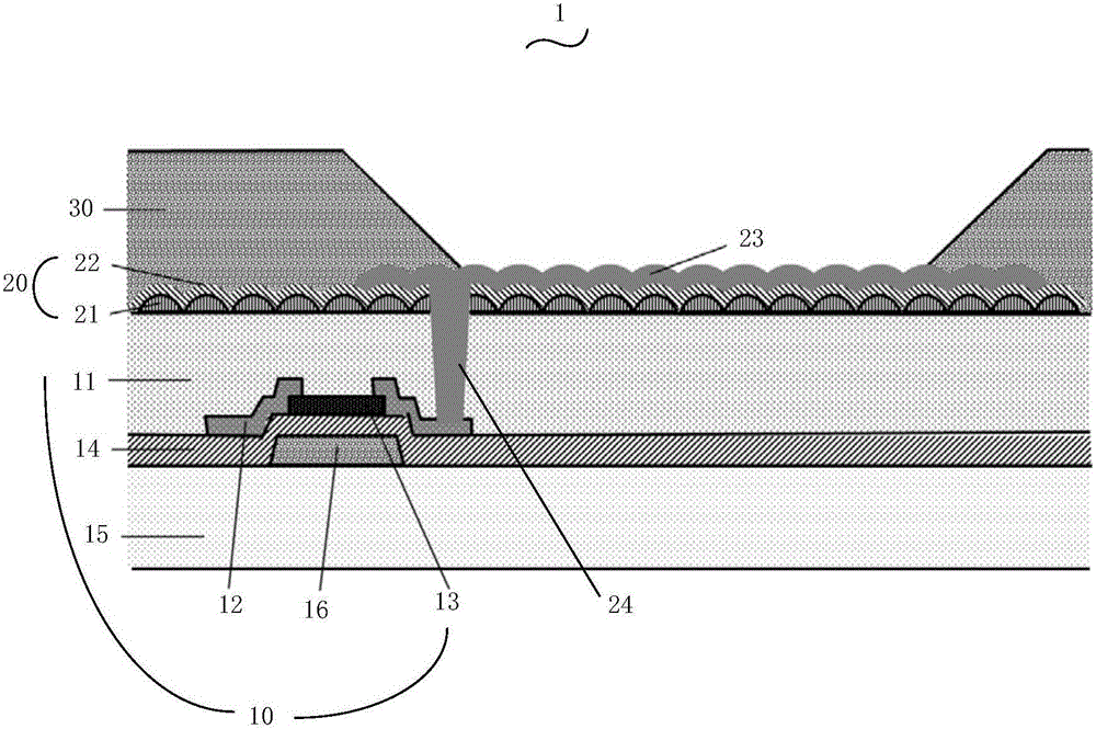
[0025] see figure 1 , is a structural schematic diagram of the pixel structure of the present invention. Such as figure 1 As shown, the pixel structure 1 includes a stacked thin film transistor array pattern unit 10 and a pixel pattern unit 20, the pixel pattern unit 20 includes a wrinkled thin film layer 21 on the thin film transistor array pattern unit 10, covering the The protective layer 22 on the wrinkled film layer 21 , the pixel electrode layer 23 located on the protective layer 22 and electrically connected to the thin film transistor array pattern unit 10 and the light-emitting defined area 30 .

[0026] Wherein, the thin film transistor array pattern unit 10 includes a flat layer 11 supporting the wrinkled thin film layer, a source pattern and a drain pattern 12 arranged on the flat layer 11 and spaced from each other, electrically connected to the The active layer 13 between the source pattern and the drain pattern 12, the gate insulating layer 14 covering the act...


PUM


Abstract

The invention discloses a pixel structure, a manufacturing method and a display panel. The pixel structure comprises a thin film transistor array pattern unit and a pixel pattern unit which are arranged in a laminated manner, wherein the pixel pattern unit comprises a wrinkle structure thin film layer positioned on the thin film transistor array pattern unit, a protective layer with which the wrinkle structure thin film layer is covered, and a pixel electrode layer which is positioned on the protective layer and is electrically connected to the thin film transistor array pattern unit and a light-emitting definition area so as to improve the light extraction efficiency of a light-emitting device, and then the device performance is improved, the power consumption of the display panel is reduced, and the service life is prolonged.

Description

technical field [0001] The invention relates to the field of display technology, in particular to a pixel structure, a manufacturing method and a display panel. Background technique [0002] Currently, the importance of displays as a visual information transmission medium is further enhanced, and in order to dominate in the future, displays are trending towards lighter, thinner, lower power consumption, lower cost, and better image quality. Organic light-emitting diodes (OLEDs) are promising in the industry for their potential market prospects due to their advantages of self-luminescence, fast response, wide viewing angle, high brightness, and thinness. The advantages of high luminous quantum efficiency and easy adjustment of luminous color have become a strong competitor of OLED in recent years. These two display technologies are the two main directions of development in the display field. However, limited by the light loss inside the device structure, only about 20% of th...

Claims


Application Information

Patent Timeline
Patent Type & Authority Applications(China)
IPC IPC(8): H01L27/12H01L21/77H01L27/32
CPCH01L27/1218H01L27/1262H10K59/121H01L25/0753H10K59/123H10K59/124H10K59/122H10K50/858H10K59/879H10K50/115H10K59/1201H10K59/1213H01L21/31111H01L23/5226H01L27/1248H01L27/156H01L29/42384H01L29/78618H01L33/06
Inventor 史文
Owner TCL CHINA STAR OPTOELECTRONICS TECH CO LTD
Why Eureka
Try Eureka