Novel bending micro-strip ridge substrate integrated gap waveguide structure

A gap waveguide and bending technology, applied in the field of electronics, can solve problems such as no public reports, and achieve the effect of solving discontinuity problems, stable structure, and good transmission performance

Active Publication Date: 2016-11-09
YUNNAN UNIV
View PDF2 Cites 12 Cited by
  • Summary
  • Abstract
  • Description
  • Claims
  • Application Information

AI Technical Summary

Problems solved by technology

[0008] Contents of the present invention, through literature search, do not see the public report identical with the present invention

Method used


Image

  • Novel bending micro-strip ridge substrate integrated gap waveguide structure
  • Novel bending micro-strip ridge substrate integrated gap waveguide structure
  • Novel bending micro-strip ridge substrate integrated gap waveguide structure

Examples


Embodiment Construction

[0027] The technical solutions of the present invention will be further described in detail below in conjunction with specific embodiments.

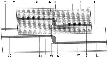
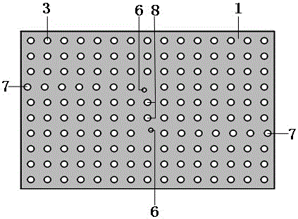
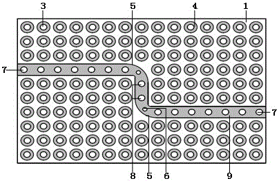
[0028] Such as Figure 1-6 As shown, a novel curved microstrip ridge substrate integrated gap waveguide structure, including: a via layer dielectric plate 1, a gap layer dielectric plate 2, wherein:

[0029] A metal layer is printed on the upper surface of the via layer dielectric board 1; a first arc-curved microstrip line 9 is arranged laterally in the middle of the lower surface, and the first microstrip line 9 adopts an arc-curved design. The first via hole 7 is provided, the two circular arc curved sections 5 are respectively provided with micro via holes 6, and the vertical section between the two arc curved sections 5 is provided with a second through hole 8, and the diameter of the micro via hole 6 is smaller than that of the first via hole. The first via hole 7 is small, the arc bending design and the via hole 6 solve the probl...


PUM


Abstract

The invention relates to a novel bending micro-strip ridge substrate integrated gap waveguide structure. In a double-layer dielectric plate bending micro-strip ridge substrate integrated gap waveguide formed by bonding a via hole layer dielectric plate and a gap layer dielectric plate, a metal layer is printed on the upper surface of the via hole layer dielectric plate, an arc bending first micro-strip line is arranged on the lower surface of the via hole layer dielectric plate, the first micro-strip line adopts an arc bending design, a first via hole, a second via hole, a micro via hole and a first micro-strip line form a bending micro-strip ridge structure, a plurality of periodical via holes are uniformly formed in two sides of the bending micro-strip ridge structure respectively, a metal circular patch is arranged under the periodical via holes, an arc bending second micro-strip line is arranged on the upper surface of the gap layer dielectric plate, a first gradual change line and a second gradual change line are arranged at two ends of the second micro-strip line respectively, and a metal layer is printed on the lower surface of the gap layer dielectric plate. According to the structure, the problems of bending discontinuity and cavity resonance are solved, and meanwhile, the structure has the advantages of simple structure, easy integration, simple processing, small size, wide broadband, low loss and structure stability and the like.

Description

technical field [0001] The invention relates to the field of electronic technology, in particular to a novel curved microstrip ridge substrate integrated gap waveguide structure. Background technique [0002] Millimeter-wave monolithic integrated circuits have the advantages of small size, high reliability, and ease of large-scale production, and their applications are becoming more and more extensive. In order to adapt to the characteristics of millimeter-wave monolithic integrated circuits, substrate-integrated gap waveguides have recently been proposed. In the substrate-integrated gap waveguide structure, electromagnetic waves can only propagate along the microstrip ridge composed of microstrip lines and metal vias, and the microstrip line is the main transmission structure. Substrate-integrated gap waveguides are fabricated using low-cost printed circuit board (PCB) processes, with figures of merit approaching that of non-planar waveguide structures. [0003] Microstri...

Claims


Application Information

Patent Timeline
Patent Type & Authority Applications(China)
IPC IPC(8): H01P3/08
CPCH01P3/088
Inventor 申东娅张秀普张晶董明袁洪
Owner YUNNAN UNIV
Why Eureka
Try Eureka