
Rectifier

A rectifier and rectifier circuit technology, applied in the electronic field, can solve problems such as high minimum input voltage, limit the working range of radio frequency identification or sensor network, etc., achieve the effect of reducing the minimum input voltage, improving power conversion efficiency, and increasing body effect

Active Publication Date: 2016-11-09
SOUTH UNIVERSITY OF SCIENCE AND TECHNOLOGY OF CHINA
View PDF2 Cites 3 Cited by
  • Summary
  • Abstract
  • Description
  • Claims
  • Application Information

AI Technical Summary

Problems solved by technology

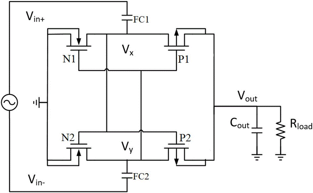
[0005] Since the rectifier of the traditional structure can only be turned on when Vy-Vx is greater than the threshold voltage, the minimum input voltage is very high
At the same time, because the rectifier of the traditional structure is difficult to be biased into the saturation region under low voltage conditions, it greatly limits the working range of radio frequency identification or sensor networks.

Method used


Image

  • Rectifier
  • Rectifier
  • Rectifier

Examples


Embodiment 1

[0038] The rectifier provided by the present invention can be a single-stage rectifier or a multi-stage rectifier, which is suitable for low input voltage, can reduce the minimum input voltage of the rectifier, and improve the power conversion efficiency of the rectifier when the ultra-low voltage is input.

[0039] Specifically, the rectifier of the present invention includes at least a single-stage rectification circuit.

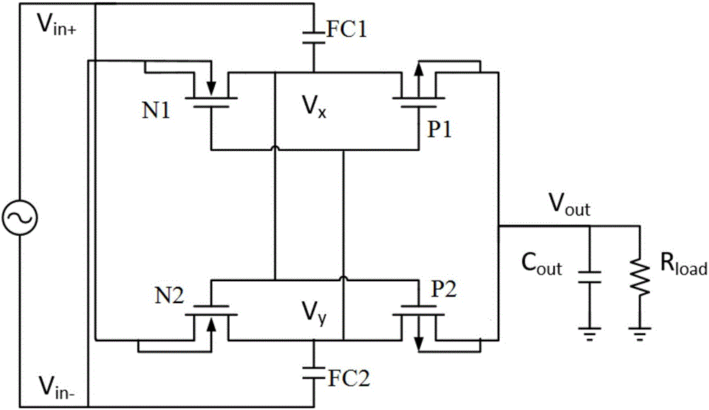
[0040] Wherein, the single-stage rectification circuit includes a first flying capacitor, a second flying capacitor, a first NMOS transistor, a second NMOS transistor, a first PMOS transistor, a second PMOS transistor and an output capacitor;

[0041] The substrate and the source of the first NMOS transistor are electrically connected to the second output end of the preceding stage circuit, and are insulated from the first output end of the preceding stage circuit, and the gate and the gate of the first PMOS transistor are electrically connected to the seco...

Embodiment 2

[0055] Figure 6 It is a circuit diagram of the multi-stage rectifier provided by Embodiment 2 of the present invention. The difference between this embodiment and Embodiment 1 is that the rectifier in this embodiment is a multi-stage rectifier. Such as Figure 6 As shown, the multi-stage rectifier may include a single-stage rectification circuit and a multi-stage AC boost circuit. In this embodiment, the front-stage circuit is a final-stage AC boost circuit in a multi-stage AC boost circuit.

[0056] Wherein, the single-stage rectification circuit in this embodiment is the same as that in Embodiment 1, and the multi-stage AC boosting circuit may include a first-stage AC boosting circuit and a second-stage AC boosting circuit.

[0057] The first stage AC boost circuit includes the third flying capacitor FC3, the fourth flying capacitor FC4, the third NMOS transistor N3 and the fourth NMOS transistor N4; the second stage AC boost circuit includes the fifth flying capacitor F...


PUM


Abstract

The invention discloses a rectifier which at least comprises a single-stage rectification circuit, wherein the single-stage rectification circuit comprises a first flying capacitor, a second flying capacitor, a first NMOS transistor, a second NMOS transistor, a first PMOS transistor, a second PMOS transistor and an output capacitor, wherein a substrate and a source electrode of the first NMOS transistor are electrically connected to a second output end of a pre-stage circuit and are insulated from a first output end of the pre-stage circuit, a substrate and a source electrode of the second NMOS transistor are electrically connected to a first output end of a pre-stage circuit and are insulated from a second output end of the pre-stage circuit, a second end of the first flying capacitor is electrically connected with a positive end of a signal source, and a second end of the second flying capacitor is electrically connected to a negative end of the signal source; a substrate and a source electrode of the first PMOS transistor and a substrate and a source electrode of the second PMOS transistor are electrically connected and serve as an output end of the single-stage rectification circuit. According to the rectifier, minimum input voltage is lowered, and power conversion efficiency of the rectifier is improved when ultra-low voltage is input.

Description

technical field [0001] The invention relates to the field of electronic technology, in particular to a rectifier. Background technique [0002] Rectifiers are widely used in RFID, wireless charging, supply chain management and wireless sensor networks. Among them, the power conversion efficiency (Power Conversion Efficiency, PCE) and the minimum input voltage largely determine the performance of the rectifier. [0003] Traditional single-stage rectifiers such as figure 1 As shown, when the input positive terminal is a positive voltage and the input negative terminal is a negative voltage, the metal oxide semiconductor field effect transistor, that is, the MOS tube, P1 and N2 are turned on, P2 and N1 are turned off, and the Vx point is at a high level , while the Vy point is charged to the ground, and the forward conduction current is output through P1. When the input negative terminal is a positive voltage and the input positive terminal is a negative voltage, P2 and N1 a...

Claims


Application Information

Patent Timeline
IPC IPC(8): H02M7/219H02M7/23
CPCH02M7/219H02M7/23
Inventor 刘阳詹陈长
Owner SOUTH UNIVERSITY OF SCIENCE AND TECHNOLOGY OF CHINA
Learn More