Band-gap reference circuit free from operational amplifier

A reference circuit, no operational amplifier technology, applied in the direction of adjusting electrical variables, control/regulation systems, instruments, etc., can solve the problems of difficulty in obtaining reference voltage with low temperature coefficient, performance degradation of operational amplifier A, and affecting the accuracy of reference voltage, etc. Achieve the effects of simple structure, lower temperature coefficient, and simplified circuit structure

Active Publication Date: 2018-05-15
拓尔微电子股份有限公司
View PDF4 Cites 10 Cited by
  • Summary
  • Abstract
  • Description
  • Claims
  • Application Information

AI Technical Summary

Problems solved by technology

[0006] The traditional bandgap reference voltage source circuit usually uses an operational amplifier A to ensure that the potentials of M and N are equal. However, this method has the following disadvantages: (1) The performance of the operational amplifier A will decrease with the change of temperature; (2) The offset voltage of op amp A affects the reference voltage V REF (3) The minimum operating voltage of the operational amplifier A limits the minimum input voltage of M and N points, which increases the power consumption of the circuit; (4) The base-emitter voltage V of the triode BE It has no linear relationship with temperature, including not only first-order items, but also several higher-order items, while the traditional bandgap reference voltage source circuit only compensates for temperature-related first-order items or part of high-order items, and it is difficult to obtain a low temperature coefficient The reference voltage

Method used


Image

  • Band-gap reference circuit free from operational amplifier
  • Band-gap reference circuit free from operational amplifier
  • Band-gap reference circuit free from operational amplifier

Examples


Embodiment 1

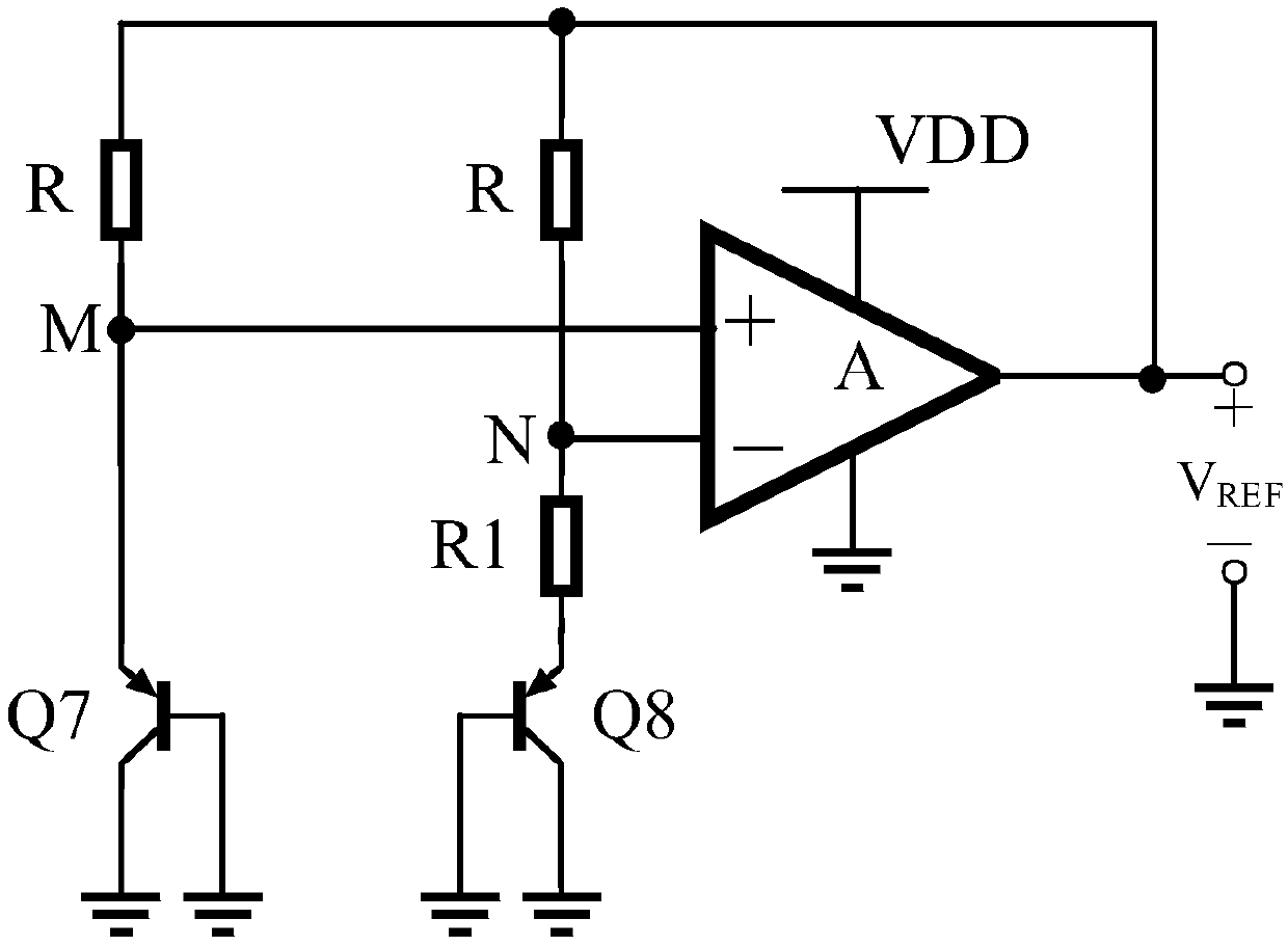
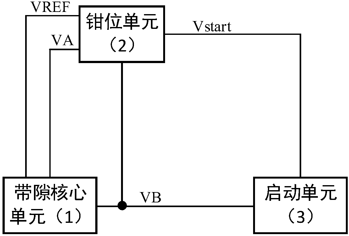
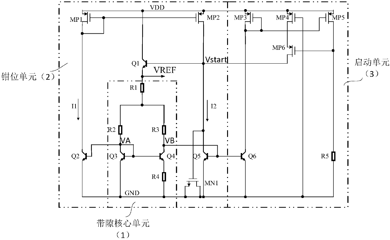
[0028] refer to figure 2 , the present invention includes: a bandgap core unit 1, a clamp unit 2 and a start unit 3; wherein the bandgap core unit 1 is provided with three output terminals, and its first output terminal outputs a clamp voltage VB; its second output terminal outputs a clamp voltage Bit voltage VA; its third output terminal outputs zero temperature coefficient reference voltage VREF. The clamping unit 2 is provided with three input terminals and one output terminal; its first input terminal is connected to the clamping voltage VA, its second input terminal is connected to the clamping voltage VB, and its third input terminal is connected to the start signal Vstart; its output terminal is connected to The zero temperature coefficient reference voltage VREF constitutes a negative feedback loop. The starting unit 3 is provided with an input terminal and an output terminal, the input terminal is connected to the clamp voltage VB; the output terminal outputs the st...

Embodiment 2

[0049] The bandgap core unit 1 and the clamp unit 2 of the present invention are the same as those in the first embodiment.

[0050] The above starting unit 3 includes a third PMOS transistor MP3, a fourth PMOS transistor MP4, a fifth PMOS transistor MP5, a sixth PMOS transistor MP6, a sixth NPN transistor Q6 and a fifth resistor R5; wherein: the third PMOS transistor MP3 and the fifth resistor R5 PMOS transistor MP5, its gate is connected to form a current mirror structure, and its source is connected to the power supply voltage VDD; the drain of the third PMOS transistor MP3 is connected to its own gate and connected to the collector of the sixth NPN transistor Q6; The drain of the fifth PMOS transistor MP5 is connected to GND through the fifth resistor R5; the emitter of the sixth NPN transistor Q6 is connected to GND, and its base is connected to the clamp voltage VB as the input terminal of the startup unit 3; the fourth PMOS transistor MP4 is connected to the gate of the...


PUM


Abstract

The invention discloses a band-gap reference circuit free from an operational amplifier. The band-gap reference circuit comprises a band gap core unit, a clamp unit and a starting unit; the band gap core unit is used for generating zero temperature coefficient reference voltage VREF; the input end of the clamp unit is connected with clamp voltage VA and clamp voltage VB, and an output end is connected with the reference voltage VREF and formed to be a negative feedback along with the band gap core unit; the clamp unit is used for guaranteeing that the clamp voltage VA and clamp voltage VB output by the band gap core unit are equal to each other; an input end of the starting unit is connected with the clamp voltage VB, and an output end outputs a starting signal Vstart to the clamp unit forguaranteeing that the clamp unit and the band gap core unit can rapidly enter a normal working state in the process of electrifying. For not adopting the operational amplifier structure, the influence of offset voltage on the reference voltage VREF is weakened, and the temperature coefficient of the reference voltage is reduced by a resistance proportional compensation technology. The band-gap reference circuit is featured by low temperature offset, low power consumption, and simple structure; the band-gap reference circuit can be applied to a chip with high requirement on static power consumption.

Description

technical field [0001] The invention belongs to the technical field of electronic circuits, in particular to a bandgap reference circuit without an operational amplifier, which can be used in power management chips. Background technique [0002] The reference voltage source is an indispensable unit module in analog circuits and digital-analog hybrid circuits, and is widely used in the design of integrated circuits such as high-precision power management chips, AD / DA converters, and random dynamic memories. Among many reference circuit structures, the bandgap reference voltage source has become the most widely used reference voltage source technology because of its ability to provide accurate voltage and high temperature stability. [0003] refer to figure 1 , the basic principle of the traditional bandgap reference voltage source circuit is to add two voltage signals with opposite temperature coefficients according to a certain ratio to obtain a temperature-independent refe...

Claims


Application Information

Patent Timeline
Patent Type & Authority Applications(China)
IPC IPC(8): G05F1/567
Inventor 来新泉王慧王宇恒李琴琴
Owner 拓尔微电子股份有限公司
Why Eureka
Try Eureka