Voltage deviation correction device and method
A technology of voltage offset and correction device, applied in the direction of electrical components, multiple input and output pulse circuits, pulse processing, etc., can solve the problems of increasing power consumption, increasing circuit area, additional amplifiers and storage capacitors, etc., to reduce voltage Offset, the effect of reducing the voltage offset
- Summary
- Abstract
- Description
- Claims
- Application Information
AI Technical Summary
Problems solved by technology
Method used
Image


Examples
Embodiment 1
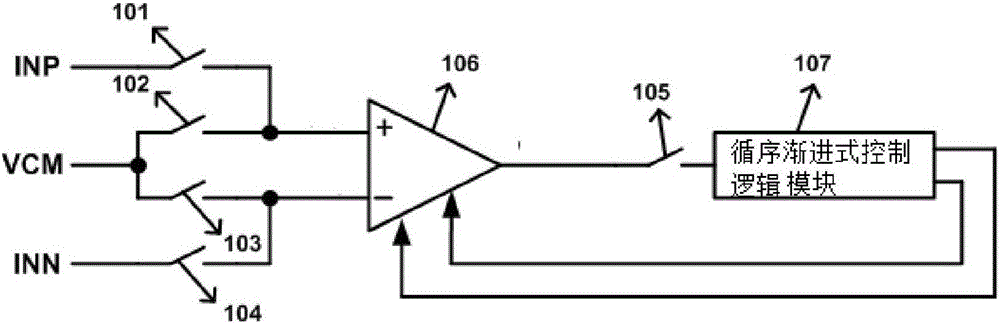
[0037] Such as figure 1 As shown, the present embodiment relates to a voltage offset correction device, which includes: a comparator or operational amplifier 106 and a step-by-step control logic module 107 connected to the comparator or operational amplifier 106, the step-by-step control logic The module 107 reduces the voltage offset of the comparator or the operational amplifier 106 by adjusting the areas of the field effect transistors at the positive and negative terminals of the comparator or the operational amplifier 106 .
[0038] In a preferred embodiment of the present invention, the above-mentioned voltage offset correction device further includes a first switching element 101, a second switching element 102, a third switching element 103, and a fourth switching element 104; between the positive input terminal of the comparator or operational amplifier 106 and the first signal input terminal INP; the second switching element 102 is arranged between the positive input...
Embodiment 2
[0045] Such as image 3 As shown, this embodiment relates to a voltage offset correction method, including the voltage offset correction device in the first embodiment above. Specifically, the method includes:
[0046] 201. Short-circuit the positive input terminal and the negative input terminal of the comparator or operational amplifier 106 .
[0047] 202, the step-by-step control logic module 107 judges whether the output voltage of the comparator or the operational amplifier 106 is a low level voltage according to the output signal of the comparator or the operational amplifier 106, if so, then enters step 203, if not, then enters step 204;
[0048] 203, the step-by-step control logic module 107 adjusts the area of the field effect transistor at the positive input end of the comparator or operational amplifier 106, and then enters step 205;
[0049] 205, the step-by-step control logic module 107 determines whether the output voltage of the comparator or the operational ...
PUM
 Abstract
Description
Claims
Application Information
 - R&D
- Intellectual Property
- Life Sciences
- Materials
- Tech Scout
- Unparalleled Data Quality
- Higher Quality Content
- 60% Fewer Hallucinations
Browse by: Latest US Patents, China's latest patents, Technical Efficacy Thesaurus, Application Domain, Technology Topic, Popular Technical Reports.
© 2025 PatSnap. All rights reserved.Legal|Privacy policy|Modern Slavery Act Transparency Statement|Sitemap|About US| Contact US: help@patsnap.com